List of Figures
Figure 1: Simplified probe input model........................................................................................................................................17
Figure 2: Input dynamic range for solder-in tips and browser..................................................................................................... 17
Figure 3: Probe setup screen panel ........................................................................................................................................... 18
Figure 4: Simplified probe architecture diagram......................................................................................................................... 24
Figure 5: Simplified drawing of input attenuation factor of the tip buffers....................................................................................25
Figure 6: Proper configuration of the Differential Input mode signal and offset voltage..............................................................26
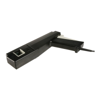
Figure 7: Solder tip measurement configuration......................................................................................................................... 27
List of Figures
P7700 Series TriMode™ Probes vi
 Loading...