Telink TLSR8232 BLE SDK Developer Handbook
AN-19112700-E1 180 Ver.1.0.0
}
The method to enable this “mask”:
Reg_irq_mask |= FLD_IRQ_SW_PWM_EN;
3) Enable MCU global interrupt “mask”, i.e. irq_enable().
10.1.10 API for IR DMA FIFO Mode
This section introduces the APIs dedicated for IR DMA FIFO mode. Please refer to PWM
demo code in the SDK.
DMA length
waveform
1
4 bytes
waveform
2
waveform
n
……
2 bytes
2 bytes
2 bytes
DMA FIFO buffer
FIFO 1
FIFO 2
FIFO n
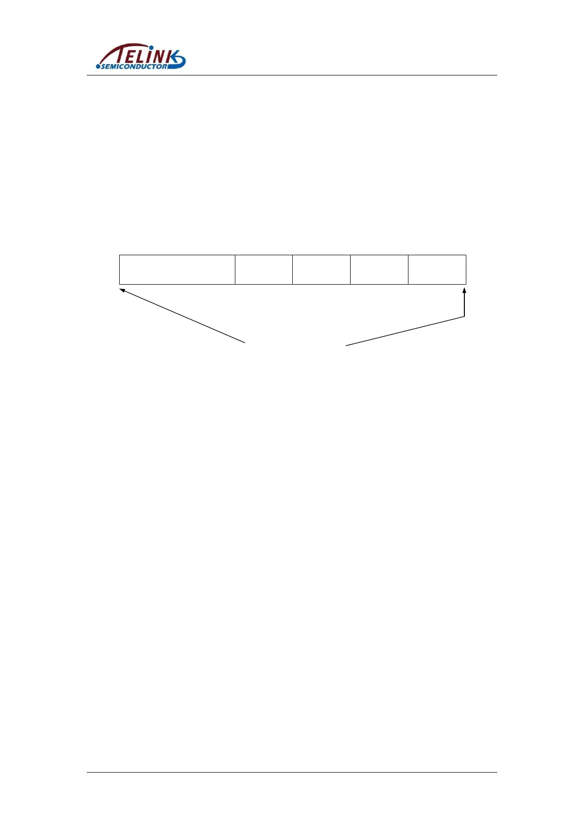
Figure 10-3 DMA FIFO Buffer for IR DMA FIFO Mode
DMA FIFO buffer is a data block defined in SRAM, and the “DMA length” of the first 4
bytes indicates the number of bytes occupied by FIFO. As shown above, DMA length =
n*2.
There are n FIFOs, and each FIFO has two bytes to indicate one PWM waveform. For
TLSR8232, “n” can be up to 256.
After DMA data buffer takes effect, PWM HW module will send out waveform 1 ~
waveform n successively.
After all waveforms are sent, PWM is stopped automatically and
IRQ_PWM0_IR_DMA_FIFO_DONE is triggered.
10.1.10.1 Configuration of DMA FIFO
Each DMA FIFO uses 2 bytes (16 bits) to configure one PWM waveform. When the API
below is called, 2-byte DMA FIFO data will be returned.
Unsigned short pwm_config_dma_fifo_waveform(int carrier_en,
Pwm0Pulse_SelectDef pulse, unsigned short pulse_num);
By configuring the three parameters “carrier_en”, “pulse” and “pulse_num”, the PWM
output waveform contains “pulse_num” PWM pulses (Signal Frames).
As shown in the configuration format in the 8232 datasheet, BIT(15) specifies Signal
Frame format of PWM waveform, and corresponds to the “carrier_en” of this API.
When “carrier_en” is 1, PWM will output carrier pulse.
When “carrier_en” is 0, PWM will output Signal Frames with low level only.