5.4 Schematic........................................................................................................................................................................ 39
6 Related Documents from Texas Instruments.....................................................................................................................43
List of Figures
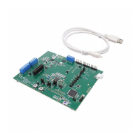
Figure 2-1. EVM Connection for Basic Operation........................................................................................................................6
Figure 3-1. Target Selection Wizard............................................................................................................................................ 8
Figure 3-2. BQStudio Window without Device.............................................................................................................................9
Figure 3-3. Register View with Device.......................................................................................................................................10
Figure 3-4. Tool Selections........................................................................................................................................................ 10
Figure 3-5. Data Memory View.................................................................................................................................................. 11
Figure 3-6. Data Memory Bit Field Change............................................................................................................................... 12
Figure 3-7. Program OTP Pane with Success Display.............................................................................................................. 13
Figure 3-8. Calibration View.......................................................................................................................................................14
Figure 3-9. Example Voltage Calibration Success.....................................................................................................................15
Figure 3-10. Example Current Calibration Failure..................................................................................................................... 15
Figure 3-11. Command Sequence View.................................................................................................................................... 16
Figure 4-1. Evaluating with Load Current.................................................................................................................................. 17
Figure 4-2. Evaluating with Charge or Discharge Current......................................................................................................... 18
Figure 4-3. Simulating Current Setup........................................................................................................................................ 18
Figure 4-4. Example 8 Cell Simple Evaluation Configuration.................................................................................................... 19
Figure 4-5. Example Connection with 9 Cells............................................................................................................................20
Figure 4-6. Host Connection Concept....................................................................................................................................... 21
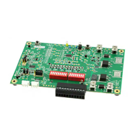
Figure 5-1. Top Silk Screen....................................................................................................................................................... 23
Figure 5-2. Top Assembly.......................................................................................................................................................... 24
Figure 5-3. Top Layer.................................................................................................................................................................25
Figure 5-4. Layer 2.................................................................................................................................................................... 26
Figure 5-5. Layer 3.................................................................................................................................................................... 27
Figure 5-6. Bottom Layer........................................................................................................................................................... 28
Figure 5-7. Bottom Silk Screen..................................................................................................................................................29
Figure 5-8. Bottom Assembly.................................................................................................................................................... 30
Figure 5-9. Schematic Diagram Monitor.................................................................................................................................... 39
Figure 5-10. Schematic Diagram Pin Configuration.................................................................................................................. 40
Figure 5-11. Schematic Diagram FETs...................................................................................................................................... 41
Figure 5-12. Schematic Diagram Interface Adapter.................................................................................................................. 42
List of Tables
Table 1-1. Ordering Information................................................................................................................................................... 3
Table 1-2. Performance Specification Summary..........................................................................................................................3
Table 4-1. Reducing Cell Count................................................................................................................................................. 19
Table 5-1. BQ76942 Circuit Module Bill of Materials................................................................................................................. 31
Table 5-2. REACH Components................................................................................................................................................ 38
Trademarks
Microsoft
®
and Windows
®
are registered trademarks of Microsoft Corporation.
All other trademarks are the property of their respective owners.
Trademarks
www.ti.com
2 BQ76942 Evaluation Module SLUUC32A – NOVEMBER 2019 – REVISED OCTOBER 2020
Submit Document Feedback
Copyright © 2020 Texas Instruments Incorporated