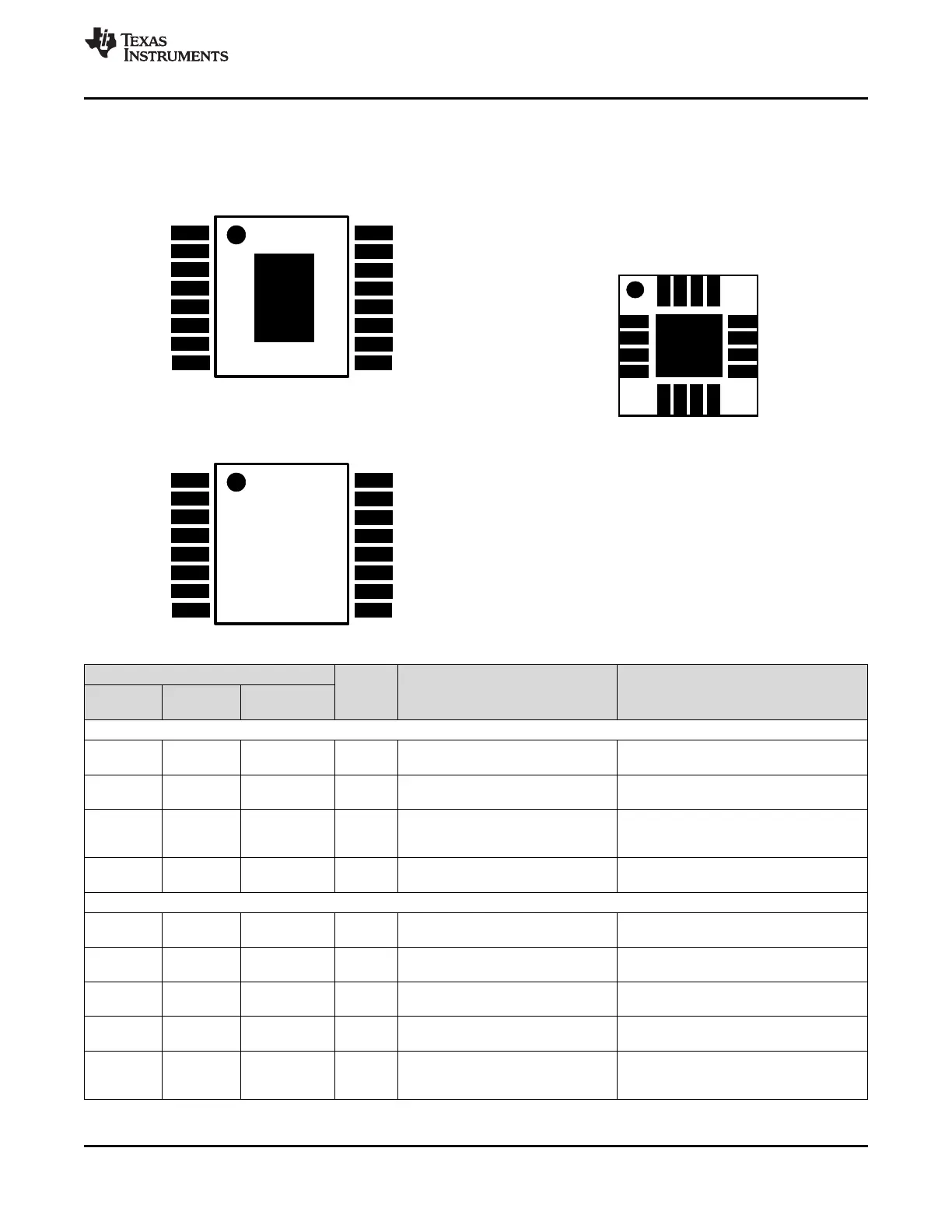
1
2
3
4
5
6
7
8
16
15
14
13
12
11
10
9
AIN1
AIN2
VINT
GND
VM
VCP
BIN2
BIN1
BOUT1
nFAULT
BOUT2
BISEN
AISEN
AOUT2
AOUT1
nSLEEP
1
2
3
4
5
6
7
8
16
15
14
13
12
11
10
9
GND
(PPAD)
AOUT1
nSLEEP
AIN1
AIN2
VINT
GND
VM
VCP
BIN1
BIN2
BOUT1
nFAULT
BOUT2
BISEN
AOUT2
AISEN
1
2
3
4
5
6
7
8
16
15
14
13
12
11
10
9
GND
(PPAD)
AIN1
AIN2
VINT
GND
VM
VCP
BIN2
BIN1
BOUT1
nFAULT
BOUT2
BISEN
AISEN
AOUT2
AOUT1
nSLEEP
DRV8833
www.ti.com
SLVSAR1E –JANUARY 2011–REVISED JULY 2015
5 Pin Configuration and Functions
PWP Package
RTY Package
16-Pin HTSSOP
16-Pin WQFN
Top View
Top View
PW Package
16-Pin TSSOP
Top View
Pin Functions
PIN
EXTERNAL COMPONENTS
I/O
(1)
DESCRIPTION
HTSSOP,
OR CONNECTIONS
NAME WQFN
TSSOP
POWER AND GROUND
11 Device ground. HTSSOP package Both the GND pin and device PowerPAD
GND 13 —
PPAD has PowerPAD. must be connected to ground.
Bypass to GND with 2.2-μF, 6.3-V
VINT 12 14 — Internal supply bypass
capacitor.
Connect to motor supply. A 10-µF
VM 10 12 — Device power supply (minimum) ceramic bypass capacitor to
GND is recommended.
Connect a 0.01-μF, 16-V (minimum) X7R
VCP 9 11 IO High-side gate drive voltage
ceramic capacitor to VM.
CONTROL
Logic input controls state of AOUT1.
AIN1 14 16 I Bridge A input 1
Internal pulldown.
Logic input controls state of AOUT2.
AIN2 13 15 I Bridge A input 2
Internal pulldown.
Logic input controls state of BOUT1.
BIN1 7 9 I Bridge B input 1
Internal pulldown.
Logic input controls state of BOUT2.
BIN2 8 10 I Bridge B input 2
Internal pulldown.
Logic high to enable device, logic low to
nSLEEP 15 1 I Sleep mode input enter low-power sleep mode and reset all
internal logic. Internal pulldown.
(1) I = Input, O = Output, OZ = Tri-state output, OD = Open-drain output, IO = Input/output
Copyright © 2011–2015, Texas Instruments Incorporated Submit Documentation Feedback 3
Product Folder Links: DRV8833