The device should then turn on and operate in open loop mode as shown in TPS7H5001-SP Output.
TPS7H50011-SP Output shows the output of TPS7H5001-SP measured on J1–J4 with the quick start method.
Figure 2-2. TPS7H5001-SP Output
The operation of this mode is such that forcing the voltage on COMP will create an output on the TPS7H5001-
SP. The duty cycle varies based on the input voltage on COMP as well as the triangle waveform created by
the CS_LIM circuit, or any other waveform that the user decides to add to the CS_LIM pin. See Duty Cycle
Generation for signal generation waveforms.
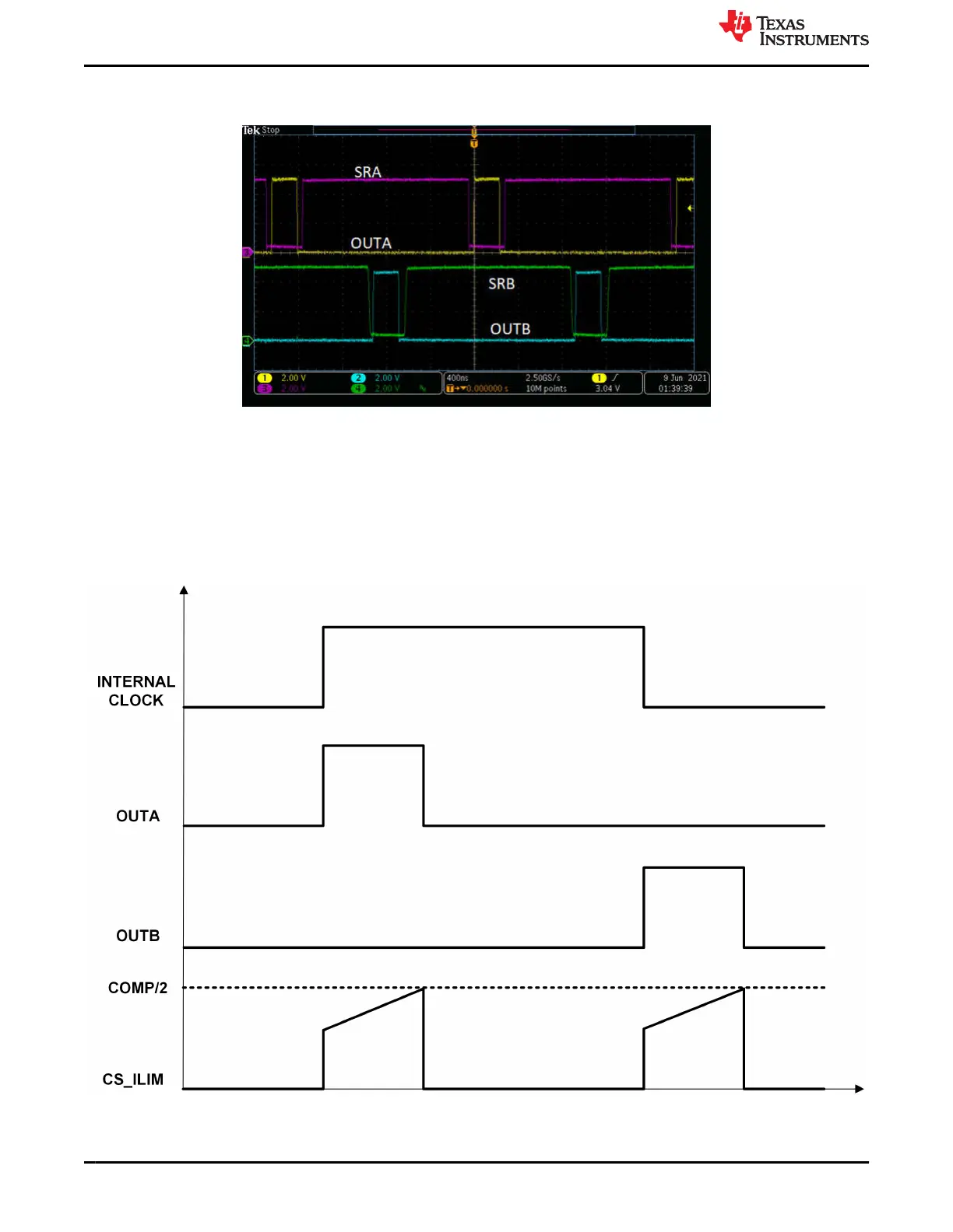
Duty Cycle Generation shows waveforms for input and output signal generations for the TPS7H5001-SP based
on COMP voltage and CS_LIM pin voltage.
Figure 2-3. Duty Cycle Generation
EVM Setup and Quick Start Guide www.ti.com
4 TPS7H5001-SP Evaluation Module SLVUBZ8 – JULY 2021
Submit Document Feedback
Copyright © 2021 Texas Instruments Incorporated

 Loading...


