NINA-B1 series - System Integration Manual
UBX-15026175 - R06 Appendix
Page 45 of 48
B.1.1 Floor plan
This section describes where the critical components and copper traces are positioned on the reference design.
Figure 17: NINA-B111 antenna reference design
Reference Part Manufacturer Description
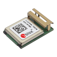
1 NINA-B111 u-blox NINA-B111 module
2 U.FL-R-SMT-1(10) Hirose Coaxial Connector, 0 – 6 GHz, for external antenna
3 Carrier PCB Should have a solid GND inner layer under and around the RF components (vias
and small openings are allowed).
4 RF trace Antenna coplanar microstrip, matched to 50 Ω
5 GND trace (Green) Minimum required top layer GND-trace.
6 Copper keep out (Dark green) Keep this area free from any copper on the top layer.
Table 13: Included parts in the antenna connector reference design
B.1.2 RF trace specification
The 50 Ω coplanar micro-strip dimensions used in the reference design are stated in Figure 18 and Table 14. The
GND plane beneath the RF trace must be intact.
Figure 18: Coplanar micro-strip dimension specification
4
1
5
2
3
6
 Loading...