NINA-B1 series - System Integration Manual
UBX-15026175 - R06 System description
Page 6 of 48
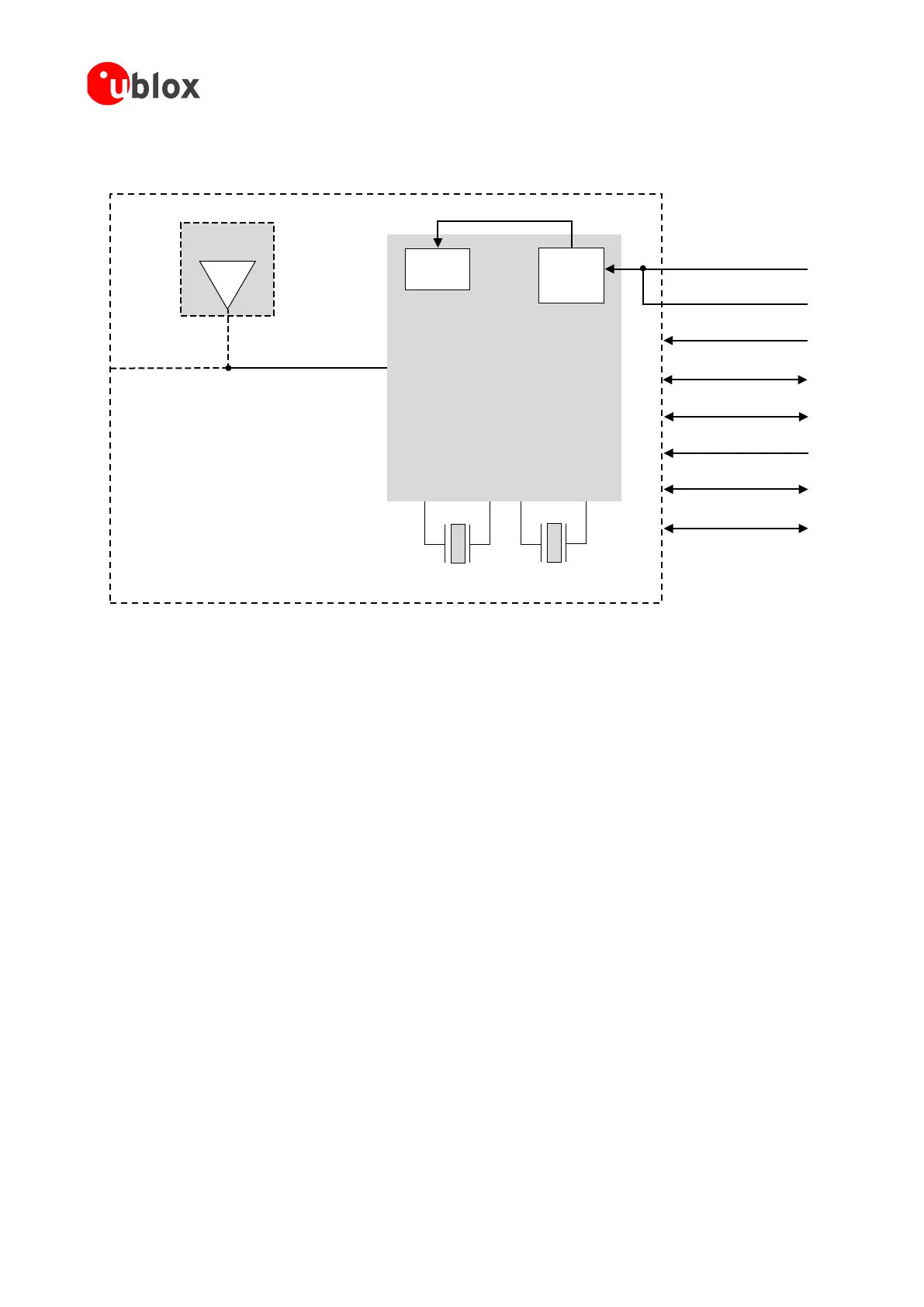
1.1.1 Module architecture
Figure 1: Block diagram of NINA-B1 series
1.1.2 Hardware options
The NINA-B1 series modules use an identical hardware configuration except for the different PCB sizes and
antenna solutions. An on board 32.768 KHz crystal is always included and an integrated DC/DC converter for
higher efficiency under heavy load situations.
1.1.3 Software options
The NINA-B1 series module can be used either together with the preflashed u-blox connectivity software or as an
Open CPU module where you can run your own application developed with either ARM mbed, Nordic SDK or
Wirepas development environment inside the NINA-B1 module. The different software options are described in
more detail in section 2.
1.2 Pin configuration and function
1.2.1 Pin attributes
1. FUNCTION: Pin function
2. PIN NAME: The name of the package pin or terminal
3. PIN NUMBER: Package pin numbers associated with each signal
4. POWER: The voltage domain that powers the pin
5. TYPE: Signal type description:
- I = Input
- O = Output
- I/O = Input and Output
- D = Open drain
- DS = Differential
- PWR = Power
- GND = Ground
Integrated
Antenna
SPI
nRF52832
Bluetooth Low Energy
RF Transceiver
with
Integrated Stacks
Application
Processor
Memory
32 MHz
DC/DC
/LDO
System
power
 Loading...