MAX-7 / NEO-7 - Hardware Integration Manual
UBX-13003704 - R09 Production Information Design
Page 22 of 52
For multi layer boards the distance between micro strip line and ground area on the top layer should at least
be as large as the dielectric thickness.
Routing the RF connection close to digital sections of the design should be avoided.
To reduce signal reflections, sharp angles in the routing of the micro strip line should be avoided. Chamfers
or fillets are preferred for rectangular routing; 45-degree routing is preferred over Manhattan style
90-degree routing.
Antenna
Antenna
Antenna
PCB
PCB
PCB
1
2
3
4
5
6
7
8
9
10
11
12
13
14
28
27
26
25
24
23
22
21
20
19
18
17
16
15
1
2
3
4
5
6
7
8
9
10
11
12
13
14
28
27
26
25
24
23
22
21
20
19
18
17
16
15
1
2
3
4
5
6
7
8
9
10
11
12
13
14
28
27
26
25
24
23
22
21
20
19
18
17
16
15
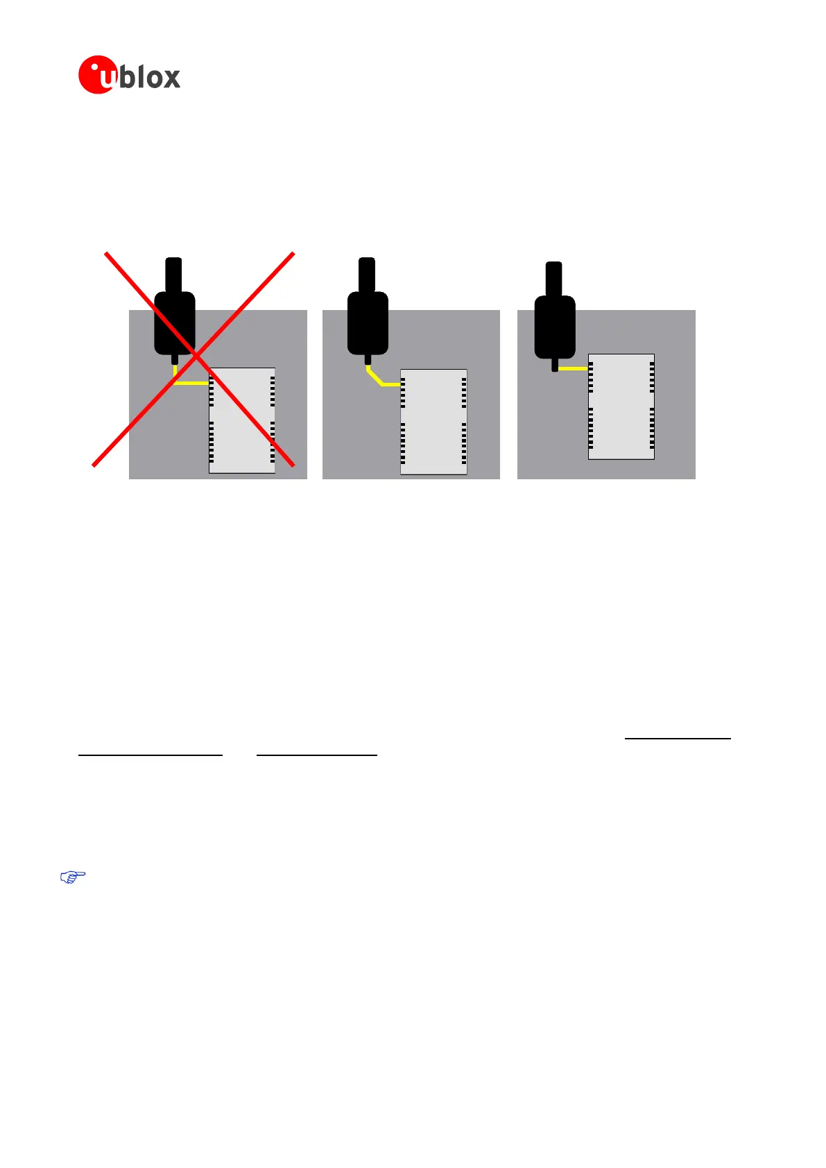
wrong better best
Figure 14: Recommended micro strip routing to RF pin
Do not route the RF-connection underneath the receiver. The distance of the micro strip line to the ground
plane on the bottom side of the receiver is very small (some 100 µm) and has huge tolerances (up to 100%).
Therefore, the impedance of this part of the trace cannot be controlled.
Use as many vias as possible to connect the ground planes.
In order to avoid reliability hazards, the area on the PCB under the receiver should be entirely covered with
solder mask. Vias should not be open. Do not route under the receiver.
3.3.5 Antenna micro strip
There are many ways to design wave-guides on printed circuit boards. A common factor to all is that calculation
of the electrical parameters is not straightforward. Freeware tools like AppCAD from Agilent or TXLine from
Applied Wave Research, Inc. are of great help in this regard. They can be downloaded from www.agilent.com or
www.hp.woodshot.com and www.mwoffice.com.
Micro strip is the most commonly used configuration on printed circuit boards and shown below in Figure 15
and Figure 16. As a rule of thumb, to achieve a 50 line impedance with FR-4 material, the width of the
conductor is roughly double the thickness of the dielectric.
Note: For the correct calculation of the micro strip impedance, one does not only need to consider the distance
between the top and the first inner layer, but also the distance between the micro strip and the adjacent GND
plane on the same layer
Use the Grounded Coplanar Waveguide model for the calculation of the line dimensions.