MAX-7 / NEO-7 - Hardware Integration Manual
UBX-13003704 - R09 Production Information Design
Page 23 of 52
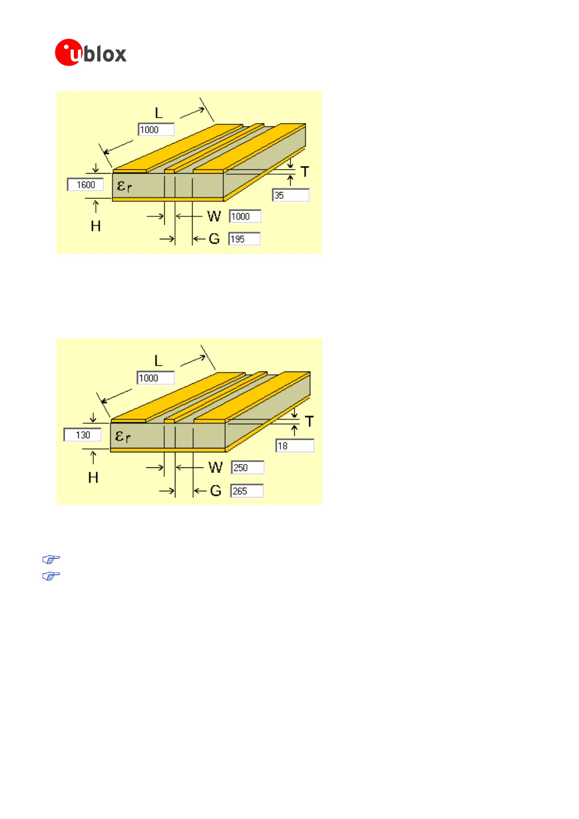
Figure 15: Micro strip on a 2-layer board (Agilent AppCAD Coplanar Waveguide)
Figure 15 shows an example of a 2-layer FR4 board with 1.6 mm thickness (H) and a 35 µm (1 ounce) copper
cladding (T). The thickness of the micro strip is comprised of the cladding (35 µm) plus the plated copper
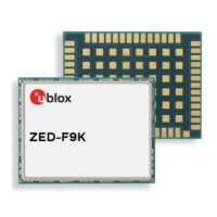
(typically 25 µm). Figure 16 is an example of a multi layer FR4 board with 18 µm (½ ounce) cladding (T) and 180
µm dielectric between layer 1 and 2.
Figure 16: Micro strip on a multi layer board (Agilent AppCAD Coplanar Waveguide)
3.4 Antenna and Antenna supervision
For all module designs shown in this section, see the data sheet for exact pin orientation.
For recomended parts, see section 3.5.
3.4.1 Antenna design with passive antenna
A design using a passive antenna requires more attention to the layout of the RF section. Typically, a passive
antenna is located near electronic components; therefore, care should be taken to reduce electrical ‘noise’ that
may interfere with the antenna performance. Passive antennas do not require a DC bias voltage and can be
directly connected to the RF input pin RF_IN. Sometimes, they may also need a passive matching network to
match the impedance to 50 .