NINA-W1 series - System integration manual
UBX-17005730 - R11 Handling and soldering Page 44 of 55
C1 - Public
Handling and soldering
No natural rubbers, hygroscopic materials or materials containing asbestos are employed.
4.1 Packaging, shipping, storage and moisture preconditioning
For information pertaining to reels, tapes or trays, moisture sensitivity levels (MSL), shipment and
storage, as well as drying for preconditioning refer to NINA-W1 series Data Sheets [2]/[3]/[4],
and u-
blox Package Information Guide [5].
4.2 Handling
The NINA-W1 series modules are Electro-Static Discharge (ESD) sensitive devices and require special
precautions during handling. Particular care must be exercised when handling patch antennas, due to
the risk of electrostatic charges. In addition to standard ESD safety practices, the following measures
should be taken into account whenever handling the receiver:
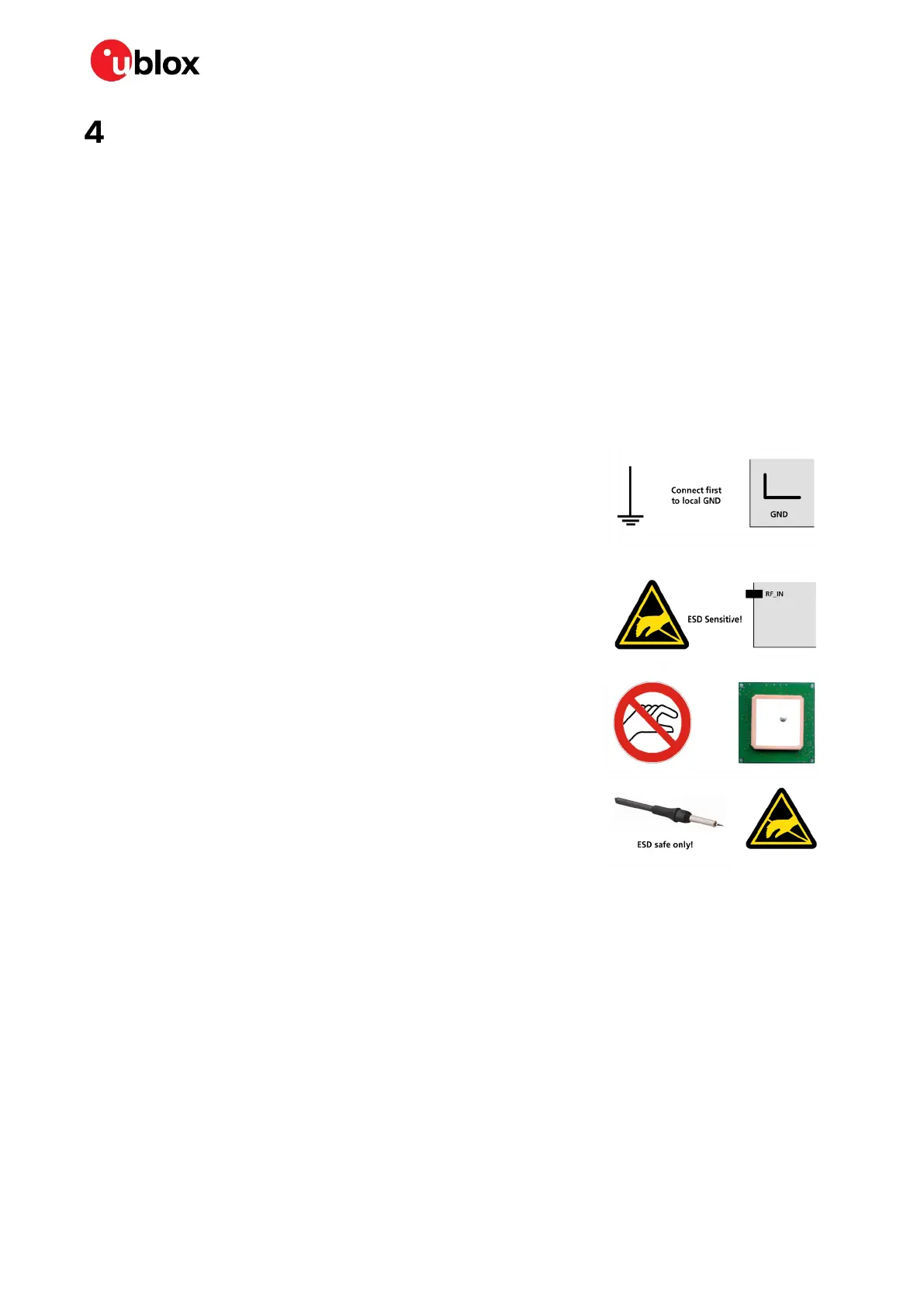
Unless there is a galvanic coupling between the local
GND (i.e. the work table) and the PCB GND, then the
first point of contact when handling the PCB must
always be between the local GND and PCB GND.
• Before mounting an antenna patch, connect ground
of the device
When handling the RF pin, do not come into contact
with any charged capacitors and be careful when
contacting materials that can develop charges (e.g.
patch antenna ~10 pF, coax cable ~50-
soldering iron, …)
To prevent electrostatic discharge through the RF
input, do not touch any exposed antenna area. If there
is any risk that such exposed antenna area is touched
in non ESD protected work area, implement proper
ESD protection measures in the design.
When soldering RF connectors and patch antennas to
the receiver’s RF pin, make sure to use an ESD safe
soldering iron (tip).
4.3 Soldering
4.3.1 Reflow soldering process
The NINA-W1 series modules are surface mount modules supplied on a FR4-type PCB with gold plated
connection pads and are produced in a lead-free process with a lead-free soldering paste. The bow
and twist of the PCB is maximum 0.75% according to IPC-A-610E. The thickness of solder resist
between the host PCB top side and the bottom side of the NINA-W1 series module must be considered
for the soldering process.
The module is compatible with industrial reflow profile for RoHS solders. Use of "No Clean" soldering
paste is strongly recommended.
The reflow profile used is dependent on the thermal mass of the entire populated PCB, heat transfer
efficiency of the oven, and particular type of solder paste used. The optimal soldering profile used has
to be trimmed for each case depending on the specific process and PCB layout.
 Loading...