SARA-G3 and SARA-U2 series - System Integration Manual
UBX-13000995 - R26 Design-in
Page 143 of 217
2.6.3.2 Guidelines for USB layout design
The USB_D+ / USB_D- lines require accurate layout design to achieve reliable signaling at the high speed data
rate (up to 480 Mbit/s) supported by the USB serial interface.
The characteristic impedance of the USB_D+ / USB_D- lines is specified by the Universal Serial Bus Revision 2.0
specification [14]. The most important parameter is the differential characteristic impedance applicable for the
odd mode electromagnetic field, which should be as close as possible to 90 differential. Signal integrity may
be degraded if PCB layout is not optimal, especially when the USB signaling lines are very long.
Use the following general routing guidelines to minimize signal quality problems:
Route USB_D+ / USB_D- lines as a differential pair.
Route USB_D+ / USB_D- lines as short as possible.
Ensure the differential characteristic impedance (Z
0
) is as close as possible to 90 .
Ensure the common mode characteristic impedance (Z
CM
) is as close as possible to 30 .
Consider design rules for USB_D+ / USB_D- similar to RF transmission lines, being them coupled differential
micro-strip or buried stripline: avoid any stubs, abrupt change of layout, and route on clear PCB area.
Avoid coupling with any RF line or sensitive analog inputs, since the signals can cause the radiation of some
harmonics of the digital data frequency.
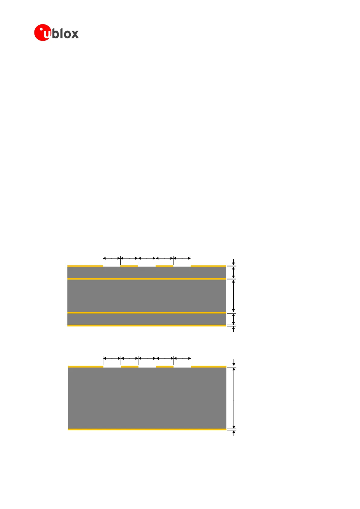
Figure 77 and Figure 78 provide two examples of coplanar waveguide designs with differential characteristic
impedance close to 90 and common mode characteristic impedance close to 30 . The first transmission line
can be implemented for a 4-layer PCB stack-up described herein, the second transmission line can be
implemented for a 2-layer PCB stack-up described herein.
35 µm
35 µm
35 µm
35 µm
270 µm
270 µm
760 µm
L1 Copper
L3 Copper
L2 Copper
L4 Copper
FR-4 dielectric
FR-4 dielectric
FR-4 dielectric
350 µm 400 µm400 µm350 µm400 µm
Figure 77: Example of USB line design, with Z
0
close to 90 and Z
CM
close to 30 , for the described 4-layer board layup
35 µm
35 µm
1510 µm
L2 Copper
L1 Copper
FR-4 dielectric
740 µm 410 µm410 µm740 µm410 µm
Figure 78: Example of USB line design, with Z
0
close to 90 and Z
CM
close to 30 , for the described 2-layer board layup

 Loading...


