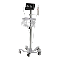
VitaScan LT
User and Service Manual
PSU:
The PSU (power supply unit) in the
IVBM-VUFE module get its input
voltage from the USB-connection.
The computer will provide all power
needed by the IVBM-VUFE module,
including motors and transducer that
are driven from this module. The power
consumption must be lower than
the maximum rating of power to be
provided by the computers USB port.
The PSU will provide 4 dierent voltages:
1.2V: FPGA
3.3V: Microcontroller,
5.0V: Analog receiver, Motor driver logic
Motor: HW-programmable voltage for
the motors to be used
USB:
The USB controller is an integral part of the
microcontroller.
The IVBM-VUFE USB will be the
SLAVE, and the computer will be
MASTER. Implementation of the USB
rmware follows the USB 2.0 standard.
Motor driver:
The motor driver is designed for running
Stepper-motors, and consists of three parts:
• A HW part that will transform logical
control signals into currents driving the
motors.
• A SW part in the microcontroller that will
keep track of position of each motor,
and generate logical control signals to
move the motors to correct positions
dependent on operating mode.
• A HW HAL-sensor and magnet to be
used as a reference to calibrate sweep-
motor position.
• The motor driver is designed to support
Full-step, Half-step and Micro-step
modes, but for maximum motor-
torque the Full-Step mode is used.
The motor supply voltage is made
HW-programmable to support dierent
step-motors.
Analog Receiver and Transmier:
The transmitter is a bipolar “square-
wave” pulse transmitter. The voltage
level is settable to tree levels by
software/conguration data control. The
waveform is controlled by a sequence
generator in the FPGA. The input signal
from the transducer is attenuated by
a t/r-switch during the pulse transmit
period. The t/r-switch is controlled by a
sequencer in the FPGA. The receiving
signal is amplied by a TGC-amplier
chain. The gain control signal is set by
an analog ramp signal, controlled from
the FPGA. The amplied analog receive
signal is low-pass ltered by a passive
L-C lter before it is fed to the A/D-
converter. The A/D converter is clocked
from the FPGA. Resolution is 12 bits,
and sampling speed is 12.5MHz. The
parallel output data is fed to the FPGA
for further digital processing.
Safety Mechanisms:
The following safety mechanisms
are implemented in the IVBM VUFE
module:
TX-Voltage and Input voltage monitoring
Soware Watchdog:
The microcontroller is supervising
the voltages in the “main loop” for
maximum safety, and a watchdog is
supervising the microcontroller program
execution.
In case of a SW/HW error that causes
abnormal program execution, a HW-
reset condition will occur and the High
Voltage will be disabled. The HW has
a measurement circuit allowing the
microcontroller to measure the High
Voltage and the Input voltage.
The microcontroller will disable the TX
Voltage if the voltage is out of the pre-
dened range (+-10% of set value), and
an error will be sent to the computer.
If the Input voltage reaches the
minimum value (4.2V), an error
message will be sent to the computer.
If the input voltage is too low to drive
the IVBM VUFE, a HW-reset condition
will occur and the High Voltage will be
disabled.
36
PAGE
www.vitacon.com