VA41620/VA41630 Evaluation Board User’s Manual
V1.0
6
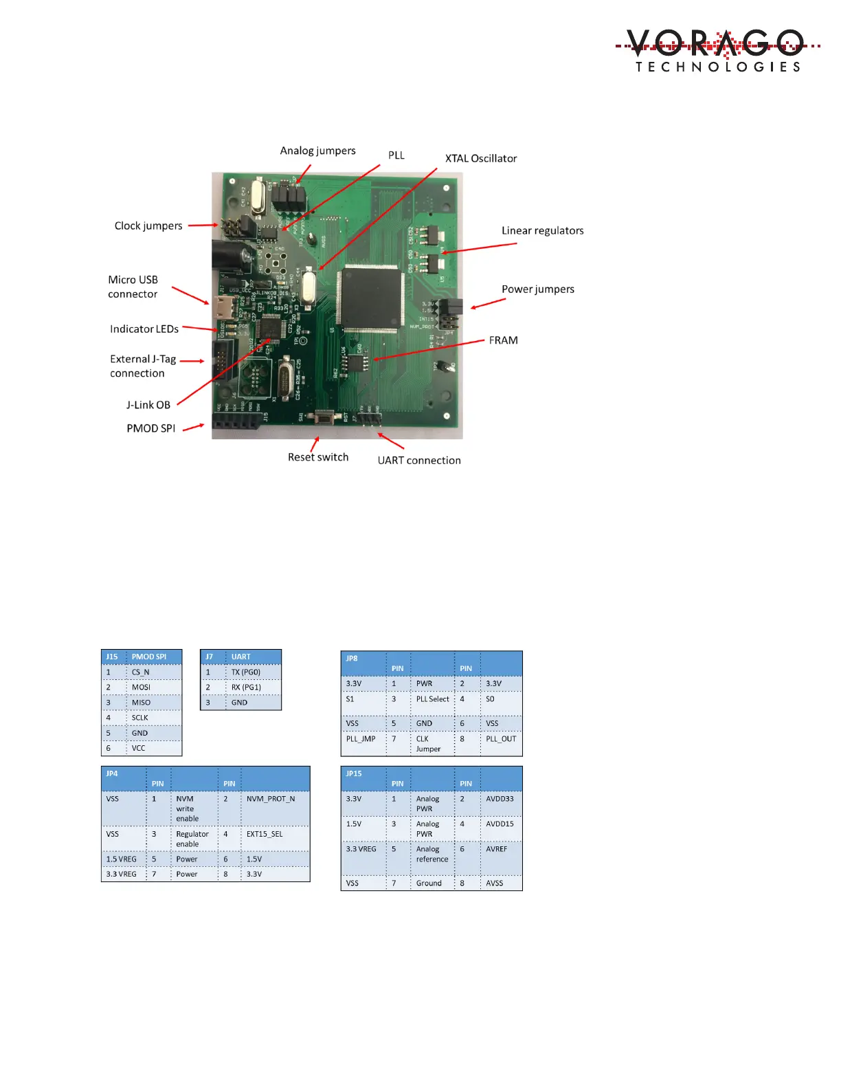
Figure 2 - Photo of PEB1 MCU board with functional circuits identified
1.5 Connector pin assignment table for MCU board
The schematics for the three boards are included in PEB1 download package. To assist with
quickly finding which pins are tied to the various connectors on the board, the following set of
tables are provided.
Table 1 - PEB1 MCU Board Connector designations
The PLL clock source provided on the MCU board is clocked with a 20MHz crystal oscillator. The
default setting on the board will provide a 40MHz clock input to the MCU. JP8 pins 7 and 8 are