VA41620/VA41630 Evaluation Board User’s Manual
V1.0
31
5.1.7 Project Build (Rebuild)
The rebuild command will compile and link all files regardless of whether they changed. Under
the Project pull-down, select Build Target.
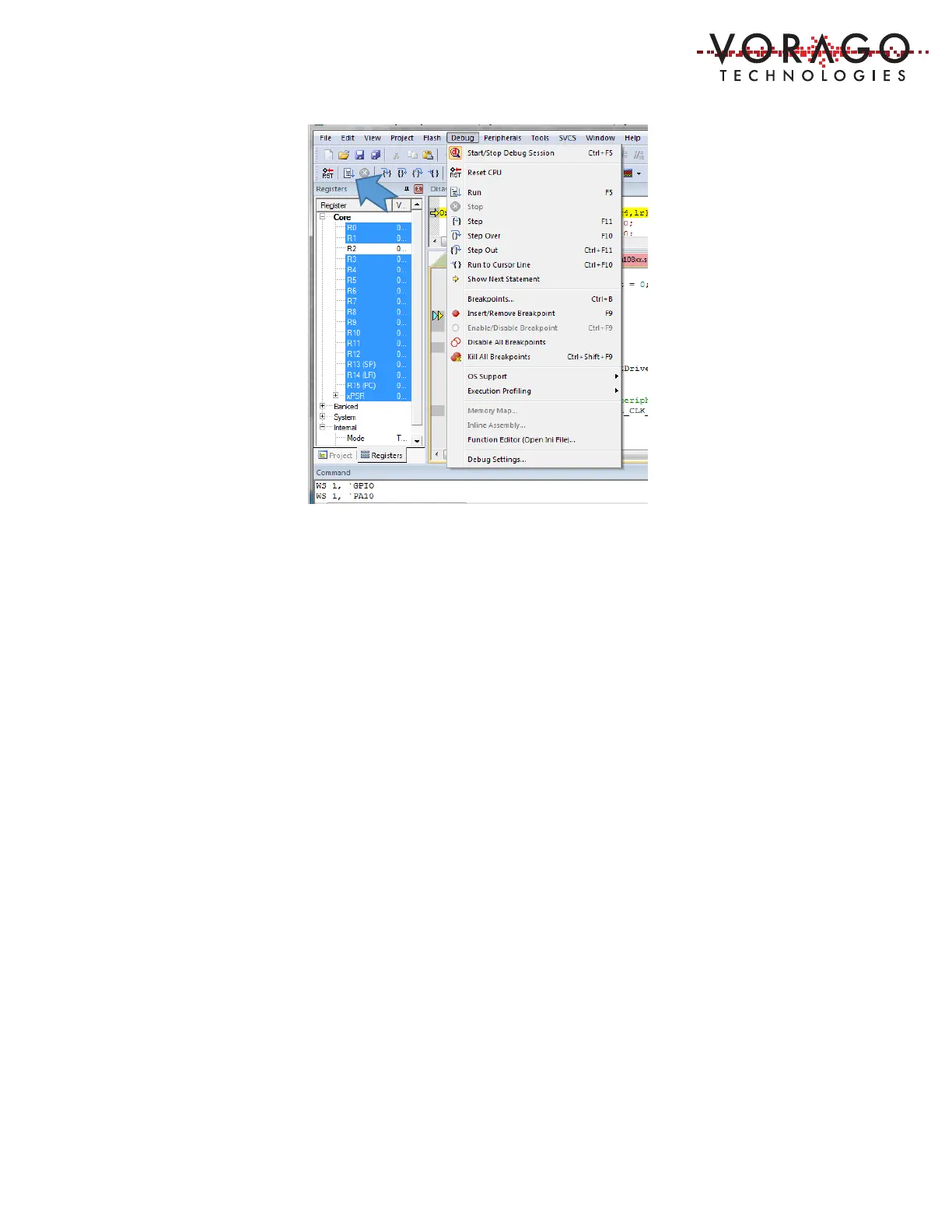
5.1.8 Download and Run
Under the Flash menu, select Download which directly loads the FRAM memory of the device.
Next, under the Debug menu, select Start/Stop Debug Session. Then under the Debug menu,
select Run
5.2 Programming procedure (Keil Specific)
The VA416xx MCUs rely on an external SPI based memory device to boot from. The 256kbyte
FRAM memory is transferred to the MCU’s program RAM automatically during the MCU boot
process by a hardware bootloader. The location of the code in the SPI memory device is the
same as the location inside the MCU. For instance, the RESET vector information is located at
address 0x0000 in both devices.
The Keil IDE provides options for programming either the flash embedded on MCUs or
connected memories such as an FRAM via the SWD port. VORAGO has provided a specific
programming algorithm for the FRAM device used on PEB1. Programming the full 256kbytes of
FRAM takes only a few seconds. Support for other SPI memories can be made available.