WM8804 Production Data
w
PD Rev 4.1 September 2007
8
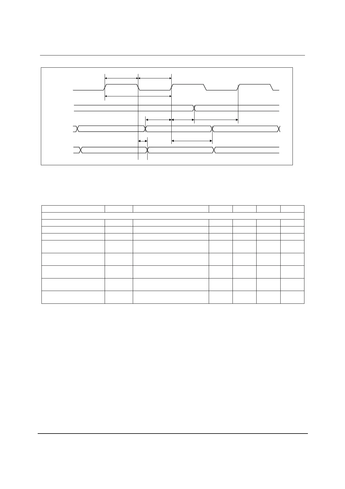
DIGITAL AUDIO INTERFACE – SLAVE MODE
BCLK
LRCLK
t
BCH
t
BCL
t
BCY
DIN
DOUT
t
LRSU
t
DS
t
LRH
t
DH
t
DD
Figure 3 Digital Audio Data Timing – Slave Mode
Test Conditions
PVDD = 3.3V, DVDD = 3.3V, PGND = 0V, DGND = 0V, T
A
= +25
o
C, fs = 48kHz, MCLK = 256fs unless stated.
PARAMETER SYMBOL TEST CONDITIONS MIN TYP MAX UNIT
Audio Data Input Timing Information
BCLK cycle time
t
BCY
50 ns
BCLK pulse width high
t
BCH
20 ns
BCLK pulse width low
t
BCL
20 ns
LRCLK set-up time to BCLK
rising edge
t
LRSU
10 ns
LRCLK hold time from
BCLK rising edge
t
LRH
10 ns
DIN set-up time to BCLK
rising edge
t
DS
10 ns
DIN hold time from BCLK
rising edge
t
DH
10 ns
DOUT propagation delay
from BCLK falling edge
t
DD
0 10 ns
Table 3 Digital Audio Data Timing – Slave Mode