Production Data WM8804
w
PD Rev 4.1 September 2007
9
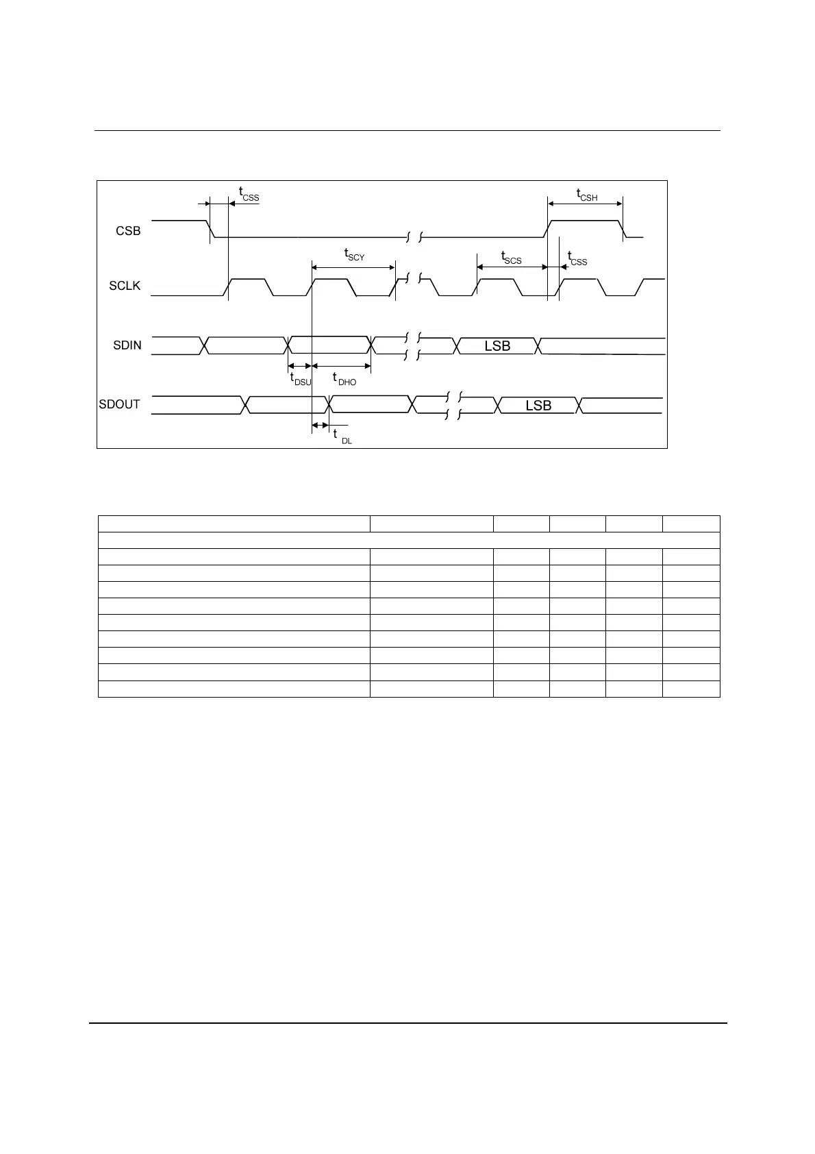
CONTROL INTERFACE – 3-WIRE MODE
Figure 4 Control Interface Timing – 3-Wire Serial Control Mode
Test Conditions
PVDD = 3.3V, DVDD = 3.3V, PGND = 0V, DGND = 0V, T
A
= +25
o
C, fs = 48kHz, MCLK = 256fs unless stated.
PARAMETER SYMBOL MIN TYP MAX UNIT
Program Register Input Information
SCLK rising edge to CSB rising edge
t
SCS
60 ns
SCLK cycle time
t
SCY
80 ns
SCLK duty cycle
40/60 60/40 %
SDIN to SCLK set-up time
t
DSU
20 ns
SDIN hold time from SCLK rising edge t
DHO
20 ns
SDOUT propagation delay from SCLK rising edge
t
DL
5 ns
CSB pulse width high
t
CSH
20 ns
CSB rising/falling to SCLK rising
t
CSS
20 ns
SCLK glitch suppression t
ps
2 8 ns
Table 4 Control Interface Timing – 3-Wire Serial Control Mode