ML605 Hardware User Guide www.xilinx.com 61
UG534 (v1.2.1) January 21, 2010
Detailed Description
J2 FMC_HPC_CLK3_M2C_P
(2)
U84.6 K4 FMC_HPC_CLK2_M2C_P
(2)
U83.6
J3 FMC_HPC_CLK3_M2C_N
(2)
U84.7 K5 FMC_HPC_CLK2_M2C_N
(2)
U83.7
J6 FMC_HPC_HA03_P AA25 K7 FMC_HPC_HA02_P AB25
J7 FMC_HPC_HA03_N Y26 K8 FMC_HPC_HA02_N AC25
J9 FMC_HPC_HA07_P AA26 K10 FMC_HPC_HA06_P AA28
J10 FMC_HPC_HA07_N AB26 K11 FMC_HPC_HA06_N AA29
J12 FMC_HPC_HA11_P AG33 K13 FMC_HPC_HA10_P AD34
J13 FMC_HPC_HA11_N AG32 K14 FMC_HPC_HA10_N AC34
J15 FMC_HPC_HA14_P AA30 K16 FMC_HPC_HA17_CC_P V30
J16 FMC_HPC_HA14_N AA31 K17 FMC_HPC_HA17_CC_N W30
J18 FMC_HPC_HA18_P T33 K19 FMC_HPC_HA21_P U31
J19 FMC_HPC_HA18_N T34 K20 FMC_HPC_HA21_N U30
J21 FMC_HPC_HA22_P U28 K22 FMC_HPC_HA23_P U26
J22 FMC_HPC_HA22_N V29 K23 FMC_HPC_HA23_N U27
J24 FMC_HPC_HB01_P AN32 K25 FMC_HPC_HB00_CC_P AF30
J25 FMC_HPC_HB01_N AM32 K26 FMC_HPC_HB00_CC_N AG30
J27 FMC_HPC_HB07_P AJ34 K28 FMC_HPC_HB06_CC_P AF26
J28 FMC_HPC_HB07_N AH34 K29 FMC_HPC_HB06_CC_N AE26
J30 FMC_HPC_HB11_P AJ29 K31 FMC_HPC_HB10_P AF28
J31 FMC_HPC_HB11_N AJ30 K32 FMC_HPC_HB10_N AF29
J33 FMC_HPC_HB15_P AE28 K34 FMC_HPC_HB14_P AE27
J34 FMC_HPC_HB15_N AE29 K35 FMC_HPC_HB14_N AD27
J36 FMC_HPC_HB18_P AD25 K37 FMC_HPC_HB17_CC_P AG27
J37 FMC_HPC_HB18_N AD26 K38 FMC_HPC_HB17_CC_N AG28
Notes:
1. Signals ending with _LS are not directly connected to the FMC HPC connector. _LS signals are connected between the listed U1
FPGA pin and a level shifter device. The signal connected between the shifted side of said device and the FMC HPC pin listed has
the same signal name, without the _LS on the end.
2. These signals do not connect to U1 FPGA pins. The pin numbers in the right-hand column identify the device and pin these signals
are connected to (U88.17 = U88 pin 17, and so on).
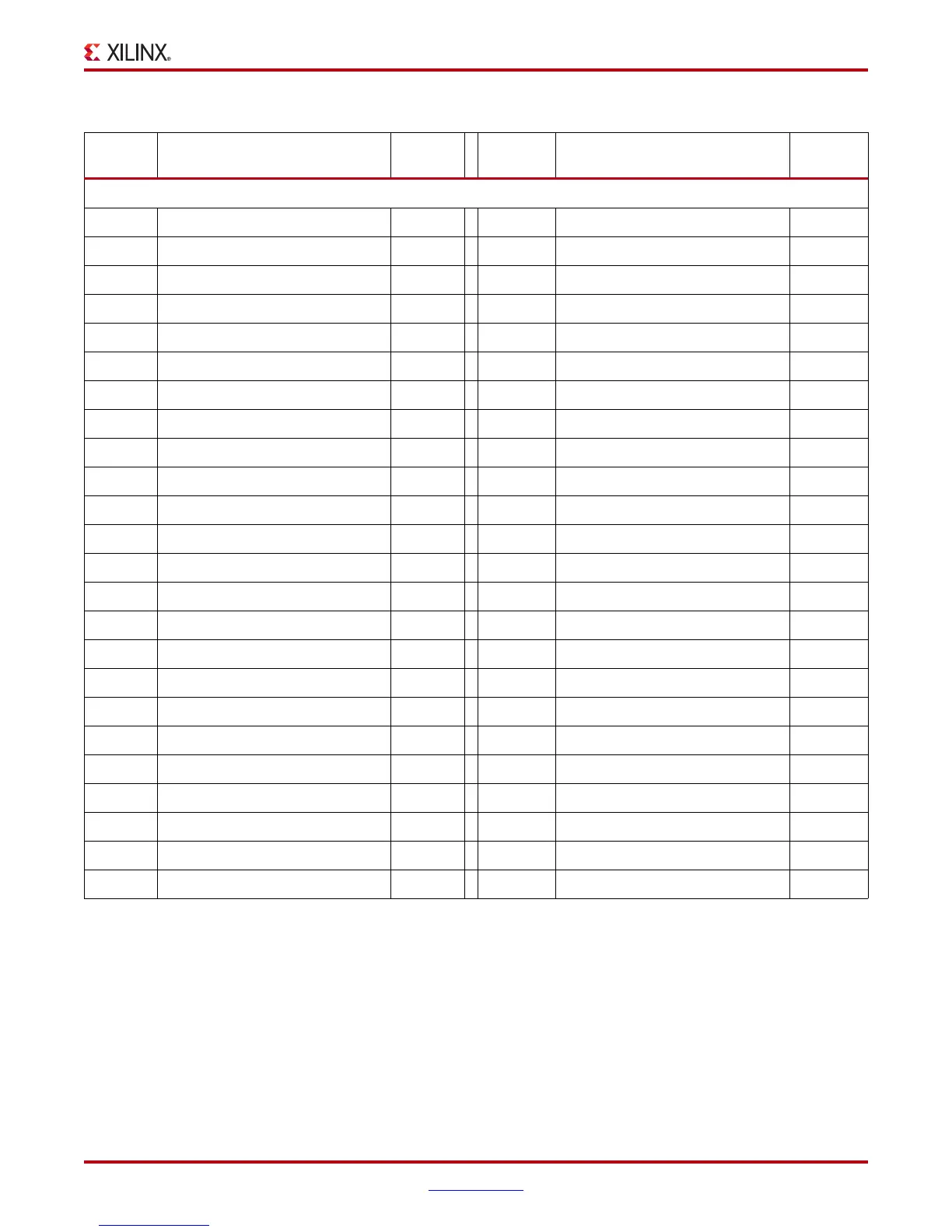
Table 1-28: VITA 57.1 FMC HPC Connections (Cont’d)
J64 FMC
HPC Pin
Schematic Net Name
U1 FPGA
Pin
J64 FMC
HPC Pin
Schematic Net Name
U1 FPGA
Pin