Do you have a question about the Xilinx ZC706 and is the answer not in the manual?
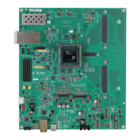
Provides a general introduction to the ZC706 evaluation board and its capabilities.
Lists the key features and components of the ZC706 evaluation board.
Details the Zynq-7000 XC7Z045 All Programmable SoC.
Describes the 1GB DDR3 SODIMM memory module on the PL side.
Explains the USB 2.0 ULPI transceiver for host computer connection.
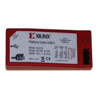
Details methods for programming the PL via JTAG.
Lists the four clock sources available for the XC7Z045 AP SoC.
Covers the 16 GTX transceivers and their connectivity.
Highlights user-accessible I/O capabilities like LEDs and pushbuttons.
Describes the board's main power slide switch (SW1).
Explains the pushbutton used to clear PL configuration.
Details the pushbuttons for PS reset functions.
Pinout and connectivity details for the High Pin Count FMC connector.
Pinout and connectivity details for the Low Pin Count FMC connector.
Details the PMBus power supply sequencer and monitor.
Describes the DC-DC voltage regulator modules.
Explains how to control the VADJ rail voltage.
Describes control over PL power rails.
Details how to monitor power rails using TI software.
Lists the default settings for the board's switches.
Lists the default positions for the board's jumpers.
Shows the pinout for the Low Pin Count FMC connector.
Shows the pinout for the High Pin Count FMC connector.
Provides Xilinx Design Constraints (XDC) for the ZC706 board.
Step-by-step guide for installing the board into a PC chassis.
Physical dimensions of the ZC706 evaluation board.
Operating temperature, storage, and humidity specifications.
Links to Xilinx support resources like Answers, Docs, Forums.
Lists external documents and websites for more information.
General statement on product conformance to EU directives.
Information on the board's CE Declaration of Conformity.
Lists relevant EU directives for the product.
Lists relevant EN and IEC standards.
Details EMC standards and product classification.
| Brand | Xilinx |
|---|---|
| Model | ZC706 |
| Category | Motherboard |
| Language | English |
