ZC706 Evaluation Board User Guide www.xilinx.com 82
UG954 (v1.5) September 10, 2015
Feature Descriptions
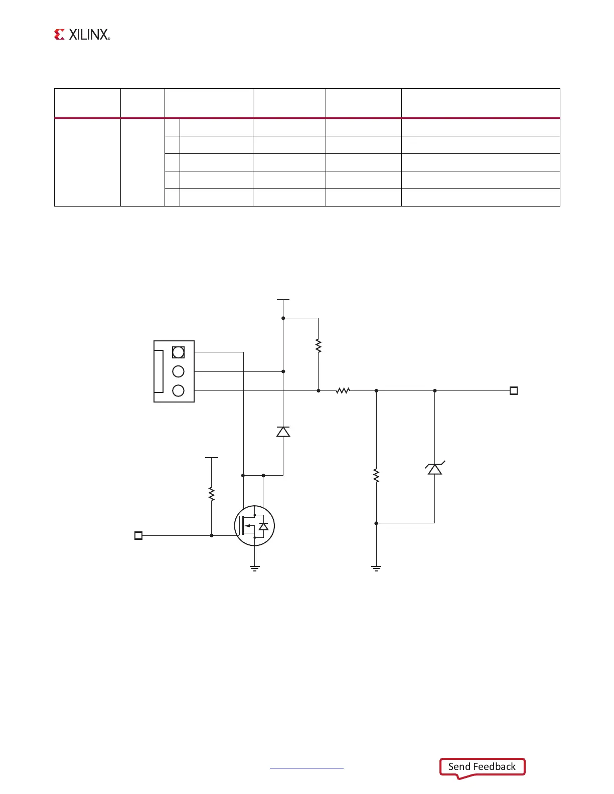
Cooling Fan
The XC7Z045 AP SoC cooling fan connector is shown in Figure 1-36.
When V
ADJ
is modified from a default of 2.5V to 1.8V or a lower V
ADJ
setting, the AP SoC U1
cooling fan turns off. Transistor Q1 is used to switch on the fan and has a max VGS of 2V,
hence the fan is not guaranteed to work at 1.8V or lower V
ADJ,
setting. See [Ref 15].
The fan turns on when the ZC706 is powered up due to pull-up resistor R369. The
SM_FAN_PWM and SM_FAN_TACH signals are wired to XC7Z045 AP SoC U1 pins AB19 and
Table 1-38: Power Rail Sequence On Dependencies for UCD90120A PMBus Controller at Address 101
Device Address Rail
Nominal
Voltage
Turn On Order Turn On Timing
UCD90120A 101d
1 VCCINT 1.000 1 Turn on at board power-on
2 VCCAUX 1.800 2 5ms after VCCINT hits 90%
5 VCC3V3_FPGA 3.300 3 5ms after VCCAUX hits 90%
3 VCC1V5_PL 1.500 4 5ms after VCC3V3 hits 90%
4 VADJ_FPGA 2.500 5 5ms after VCC1V5_PL hits 90%
X-Ref Target - Figure 1-36
Figure 1-36: Cooling Fan Circuit
SM FAN TACH
SM FAN PWM
R279
10.0K
1/10W
1%
R278
10.0K
1/10W
1%
1
2
1 2
2 4
1
3
R190
4.75K
1/10W
1%
Q1
1.3W
NDT3055L
VADJ
GND GND
J61
Keyed Fan Header
VCC12_P
R369
1.00K
1/16W
1%
1
2
1
2
D2
MM3Z2V7B
2.7V
460MW
2
1
D1
DL4148
100V
460MW
22_11_2032
1
2
1
2
3
UG954_c1_36_073013