

Do you have a question about the Xilinx ZCU102 and is the answer not in the manual?
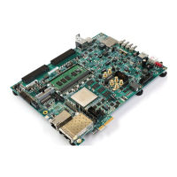
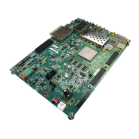
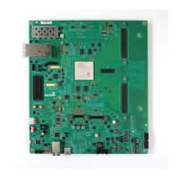
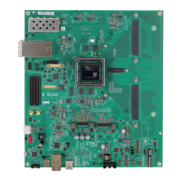
General purpose evaluation board for rapid prototyping based on the Zynq UltraScale+ XCZU9EG MPSoC.
Board component block diagram showing connections and schematic references.
Lists the key features and capabilities of the ZCU102 evaluation board.
Details physical dimensions, environmental, and operating voltage specifications.
Shows locations of components on the ZCU102 board with reference to schematic.
Provides default settings for DIP switches and jumpers on the board.
Configuration of power, mode select, and reset switches.
Default jumper settings for board configuration and overrides.
Explains boot modes (JTAG, Quad-SPI, SD) for MPSoC configuration.
Details functional descriptions of board components and features.
Description of the MPSoC device, its processing system, and logic.
Details the DDR4 SODIMM socket and installed module.
Description of the 4 Gb, 16-bit DDR4 component memory system.
Peripheral mapping of PS MIO pins on the ZCU102 board.
Details the Micron dual Quad-SPI flash memory for boot image.
Description of the USB 3.0 transceiver and USB 2.0 ULPI PHY.
Interface for SD card connection, supporting SD3.0 capabilities.
ZCU102 JTAG chain overview and connection options.
Provides trace/debug 38-pin Mictor connector connections.
Overview of fixed and variable clock sources for the MPSoC.
Details the PS reference clock generator.
Describes the I2C programmable SI570 oscillator for user clocks.
Details the programmable SI570 oscillator for MGT clocks.
Describes SMA connectors for differential MGT clock input.
PS-side Gigabit Ethernet MAC interface description.
Details the Ethernet PHY device and connections.
Describes the Ethernet PHY LED interface and its functionality.
Four level-shifted UART connections via USB connector.
GPIO bits for signaling between MPSoC and MSP430 controller.
I2C0 connections to port expanders and I2C switch.
I2C1 interface access to I2C peripherals via I2C switches.
Primary PS-side UART interface connected to CP2108 bridge.
PS-side UART1 accessed via CP2108 bridge port 1.
PS-side CAN bus TX/RX pins through level-translator and transceiver.
MIO 26 input to PMU for warm boot indication.
VESA DisplayPort 1.2 controller for main link and auxiliary channel.
PS-side PCIe reset signal wired to PCIe Gen2 x4 root port slot.
PMU output pins for power domain changes in deep-sleep mode.
High-definition multimedia interface video output using HDMI re-timer.
Details the Si5324C jitter attenuator for HDMI clock recovery.
Small form-factor pluggable connector for SFP/SFP+ modules.
Details the Si5328B jitter attenuator for SFP/SFP+ clock recovery.
Supports two PMOD GPIO headers for bank 47 connections.
2x12 male header making Bank 50 GPIO connections available.
PMOD 2x6 receptacle for I2C0 PMOD connections.
User and general purpose I/O capabilities including LEDs, switches, pushbuttons.
24 GTH gigabit transceivers on the PL-side.
PS-side GTR transceivers shared through bidirectional multiplexers.
Hosts a 4-lane PCIe root port connector.
x8 PCIe connector supporting x4 PCIe for flexibility.
Supports VITA 57.1 FMC specification with HPC connectors.
Implements a subset of full FMC HPC connectivity for HPC0.
Implements a subset of full FMC HPC connectivity for HPC1.
XCZU9EG U1 cooling fan connector, turns on when ZCU102 is powered up.
Controls VADJ_FMC power rail for FMC connectors and HP banks.
On-board MSP430 with integrated Power Advantage demo and SC firmware.
Includes power, configuration, and reset switches on the board.
Controls board power by sliding the switch actuator.
Clears programmable logic configuration when pressed.
Circuits for PS_POR_B and PS_SRST_B resets.
Details the Maxim PMBus based power system.
Monitors voltage and current via Maxim PowerTool GUI.
Shows pinout of FMC HPC connector defined by VITA 57.1 spec.
XDC file template for ZCU102 board designs.
Lists clock and DDR4 SODIMM interface constraints.
Product designed to conform to EU directives and standards.
Zynq UltraScale+ ZCU102 Declaration of Conformity is online.
Lists applicable EU directives like LVD and EMC.
EN and IEC standards maintained by CENELEC and IEC.
Information on IT equipment radio disturbance and immunity.
General requirements for IT equipment safety.
Compliance with WEEE, RoHS, and CE directives.
Links to support resources like Answers, Docs, Downloads, Forums.
Support for devices, software tools, and IP at all design stages.
Links to supplemental material and Xilinx documents.
Legal notices regarding product use and warranties.
| Processor | Quad-core ARM Cortex-A53, Dual-core ARM Cortex-R5 |
|---|---|
| SD Card | MicroSD card slot |
| Video Outputs | DisplayPort |
| FPGA | Xilinx Zynq UltraScale+ XCZU9EG-2FFVB1156E |
| Memory | 4GB DDR4 Component Memory |
| Storage | MicroSD card slot |
| Ethernet | Gigabit Ethernet |
| USB | 1 x USB 3.0, 1 x USB 2.0 |
| PCIe | PCIe Gen2 x4 |
| Display | DisplayPort |
| Power Supply | 12V DC input |
| SATA | SATA 3.0 |
| Clocking | Programmable clocks |
| Operating System Support | PetaLinux |
