ZCU102 Evaluation Board User Guide www.xilinx.com 44
UG1182 (v1.2) March 20, 2017
Chapter 3: Board Component Descriptions
SI5341B 10 Independent Output Any-Frequency Clock Generator (PS
Reference Clock)
[Figure 2-1, callout 10]
• Clock generator: Silicon Labs SI5341B-B05071-GM
• Jitter: <100 fs RMS typical
• Differential and single-ended outputs
The SI5341B is a one-time programmable clock source. For more details refer to the SI5341B
data sheet [Ref 17] for more details. The clock circuit is shown in Figure 3-8.
U69.35 GTR_REF_CLK_SATA_P
(2)
W27
U69.34 GTR_REF_CLK_SATA_N
(2)
W28
U69.31 GTR_REF_CLK_USB3_P
(2)
U27
U69.30 GTR_REF_CLK_USB3_N
(2)
U28
U69.24 GTR_REF_CLK_DP_P
(2)
U31
U69.23 GTR_REF_CLK_DP_N
(2)
U32
U42.4 USER_SI570_P
DIFF_SSTL12 AL8
U42.5 USER_SI570_N
DIFF_SSTL12 AL7
U56.4 USER_MGT_SI570_P
(2)
(1-to-2 CLOCK BUFFER) U51.6
U56.5 USER_MGT_SI570_N
(2)
(1-to-2 CLOCK BUFFER) U51.7
U51.11 USER_MGT_SI570_CLOCK1_P
(2)
L27
U51.12 USER_MGT_SI570_CLOCK1_N
(2)
L28
U51.13 USER_MGT_SI570_CLOCK2_P
(2)
C8
U51.14 USER_MGT_SI570_CLOCK2_N
(2)
C7
J79.1 USER_SMA_MGT_CLOCK_P
(2)
N27
J80.1 USER_SMA_MGT_CLOCK_N
(2)
N28
U108.28 HDMI_SI5324_OUT_P
(2)
R27
U108.29 HDMI_SI5324_OUT_N
(2)
R28
U20.28 SFP_SI5328_OUT_P
(2)
B10
U20.29 SFP_SI5328_OUT_N
(2)
B9
Notes:
1. U1 XCU9EG Bank 503 supports LVCMOS level inputs.
2. U1 MGT (I/O standards do not apply).
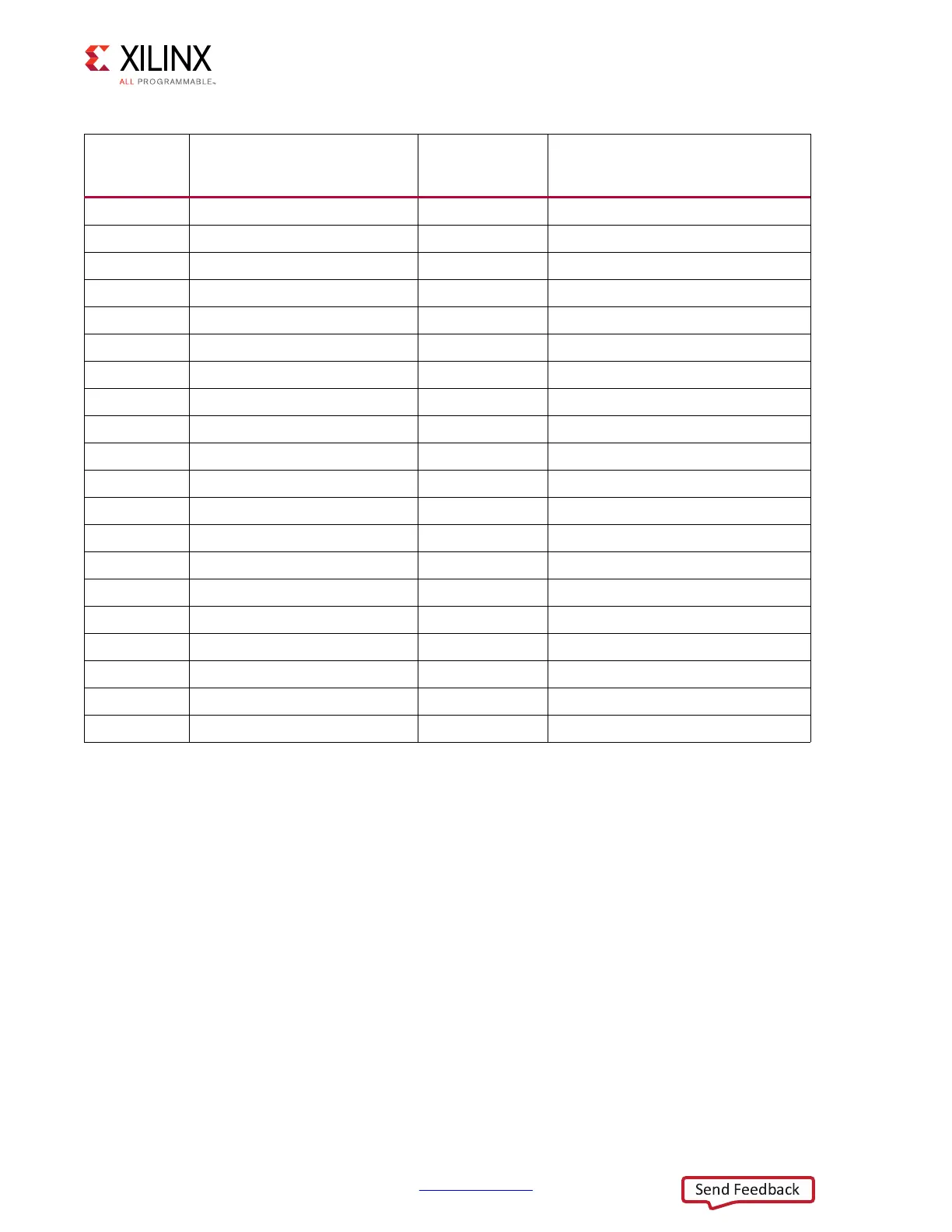
Table 3-13: Clock Connections, Source to XCZU9EG MPSoC (Cont’d)
Clock Source
Ref. Des. and
Pin
Schematic Net Name I/O Standard FPGA (U1) Pin