EasyManuals Logo

Xilinx ZCU102 User Manual

Xilinx ZCU102
137 pages
To Next Page IconTo Next Page
To Previous Page IconTo Previous Page
Page #47 background imageLoading...
Page #47 background image
ZCU102 Evaluation Board User Guide www.xilinx.com 47
UG1182 (v1.2) March 20, 2017
Chapter 3: Board Component Descriptions
User SMA MGT Clock
[Figure 2-1, callout 42]
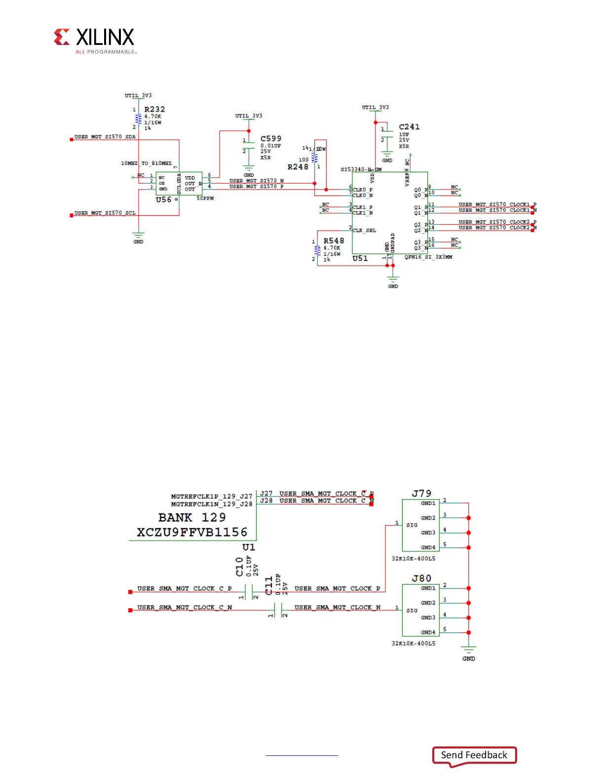
The ZCU102 board provides a pair of SMAs for differential AC coupled user MGT clock input
into FPGA U1 MGTH bank 129. This differential signal pair is series-capacitor coupled. The
P-side SMA J79 signal USER_SMA_MGT_CLOCK_P is connected to U1 MGTREFCLK0P pin J27,
with the N-side SMA J80 signal USER_SMA_MGT_CLOCK_N connected to U1 MGTREFCLK0N
pin J28. The user SMA MGT clock circuit is shown in Figure 3-11.
X-Ref Target - Figure 3-10
Figure 3-10: Programmable User MGT Clock
;
X-Ref Target - Figure 3-11
Figure 3-11: User SMA MGT Clock
;
Send Feedback

Table of Contents

Other manuals for Xilinx ZCU102

Questions and Answers:

Question and Answer IconNeed help?

Do you have a question about the Xilinx ZCU102 and is the answer not in the manual?

Xilinx ZCU102 Specifications

General IconGeneral
ProcessorQuad-core ARM Cortex-A53, Dual-core ARM Cortex-R5
SD CardMicroSD card slot
Video OutputsDisplayPort
FPGAXilinx Zynq UltraScale+ XCZU9EG-2FFVB1156E
Memory4GB DDR4 Component Memory
StorageMicroSD card slot
EthernetGigabit Ethernet
USB1 x USB 3.0, 1 x USB 2.0
PCIePCIe Gen2 x4
DisplayDisplayPort
Power Supply12V DC input
SATASATA 3.0
ClockingProgrammable clocks
Operating System SupportPetaLinux

Related product manuals