ZC706 Evaluation Board User Guide www.xilinx.com 62
UG954 (v1.5) September 10, 2015
Feature Descriptions
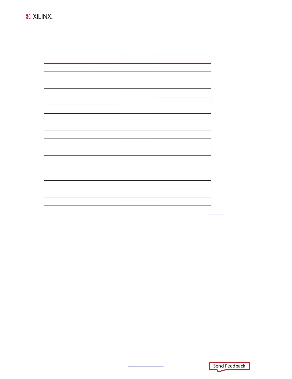
Table 1-31 lists the GPIO Header connections to XC7Z045 AP SoC U1.
See Zynq-7000 All Programmable SoC Technical Reference Manual (UG585
) for information
about the PS PJTAG functionality.
Switches
The ZC706 evaluation board includes a power and a configuration (PL PROG_B) switch:
• Power On/Off slide switch SW1 (callout 27)
• SW10 (FPGA_PROG_B), active-Low pushbutton (callout 28)
• PS System Reset Pushbuttons
Power On/Off Slide Switch
[Figure 1-2, callout 27]
The ZC706 evaluation board power switch is SW1. Sliding the switch actuator from the Off
to On position applies 12V power from J22 a 6-pin mini-fit connector. Green LED DS22
illuminates when the ZC706 evaluation board power is on. See Power Management for
details on the onboard power system.
Table 1-31: GPIO Header Connections to XC7Z045 AP SoC at U1
TCA6416APWR (U16) PORT: Pin Net Name GPIO Header J57 Pin
P00:4 IIC_PMOD_0 J57.1
P01:5 IIC_PMOD_1 J57.3
P02:6 IIC_PMOD_2 J57.5
P03:7 IIC_PMOD_3 J57.7
P04:8 IIC_PMOD_4 J57.2
P05:9 IIC_PMOD_5 J57.4
P06:10 IIC_PMOD_6 J57.6
P07:11 IIC_PMOD_7 J57.8
XC7Z045 AP SoC (U1) Pin Net Name GPIO Header J58 Pin
AJ21 PMOD1_0 J58.1
AK21 PMOD1_1 J58.3
AB21 PMOD1_2 J58.5
AB16 PMOD1_3 J58.7
Y20 PMOD1_4 J58.2
AA20 PMOD1_5 J58.4
AC18 PMOD1_6 J58.6
AC19 PMOD1_7 J58.8