ZC706 Evaluation Board User Guide www.xilinx.com 86
UG954 (v1.5) September 10, 2015
Appendix A
Default Switch and Jumper Settings
The default switch and jumper settings for the ZC706 evaluation board are provided in this
appendix.
Switches
[Figure 1-2, callout 24]
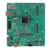
Default switch settings are listed in Table A-1. The locations of the ZC706 jumper headers
called out in Table A-2 are shown in Figure A-1.
Table A-1: Default Switch Settings
Switch Function Default Selects
Figure 1-2
Callout
SW1 Board main power On-Off Slide Switch
OFF
Delivered in OFF position
27
SW4 2-pole SPST DIP Switch, JTAG mode select
signals JTAG_SEL_[1:2]
10
JTAG = cable connector J3
34
SW11 5-pole DPDT DIP Switch, PS Boot Mode select
signals MIO[6:2]_SELECT
All Down
JTAG flat cable header J3
29
SW12 4-pole SPST DIP Switch, user signals
GPIO_DIP_SW[0:3], poles [1:4]
All OFF
All = 0 (4.7K p/d to GND)
24
 Loading...
