STE P 2I I II II II II IIII I I I I I IIII I I I I I II IIII I I I I I IIII I I I I I IIII I I I I I II IIII I I I I I II
STE P 6I I II II II II IIII I I I I I IIII I I I I I II IIII I I I I I IIII I I I I I IIII I I I I I II IIII I I I I I II
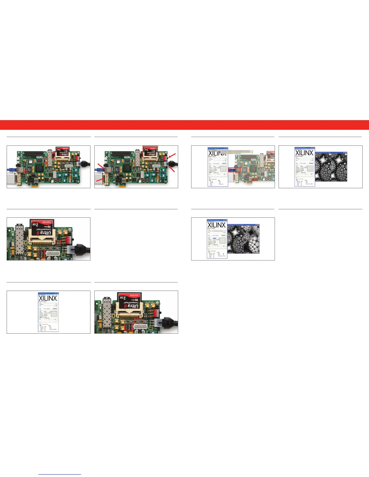
STE P 4I I II II II II IIII I I I I I IIII I I I I I II IIII I I I I I IIII I I I I I IIII I I I I I II IIII I I I I I II
STE P 8I I II II II II IIII I I I I I IIII I I I I I II IIII I I I I I IIII I I I I I IIII I I I I I II IIII I I I I I II
STE P 10I I II IIII I I I I I II IIII I I I I I IIII I I I I I IIII I I I I I IIII I I I I I II IIII I I I I I IIII I I I
Connecting Cables and CF Card
Install the CF card that is included in the kit. Connect the Ethernet cable to your PC and the
SP605 board. Connect the DVI port to a monitor (DVI2VGA adaptor included), Plug in the
power Adaptor to the local AC power. Plug the 12 volt power jack into the board connector on
J18. Turn on the power by switching the SW1 to the “ON” position.
Select an Image
On the USB FLASH there are images to select. Select the image fractal1.jpg in directory
SP601_BRD_Reference_Design --> SP601_BRD_Images. Then “Click” the “show Display”
GUI button. If you have connected a DVI or VGA monitor, you will also see this image displayed
on the monitor.
Setting Ethernet Link
In the Base Reference Design GUI Application select the menu item Setup, then select a
network. You will see the GUI indicate “Connected to FPGA” and you will see the Ethernet
Status lights active on the SP605.
Load with Base Reference Design Demo
Verify the SystemACE (S1) DIP Switch is set to “1101” where 1, 2, and 4 are set to the “ON”
position and switch 3 is set to the “OFF” position. Then press the SYSACE Reset switch (SW9)
to make sure the FPGA loads from the CF card slot 3.
Installing the Application GUI
The Base Reference Design includes an application GUI that must be installed before you will
be able to run the demo. On the USB FLASH drive, included with the kit, you will find a directory
called SP605_BRD_Reference_Design.--> SP605_BRD _Application directory. In there you
will find an install image, BaseRefDI_Setup2_0_4.msi. This is an application GUI that is used to
display the graphical information for the Base Reference Design. Please double click on this
application to install the software.
Experimenting with the Demo
As you select different filter effects, you will see that the image is filtered using these different
transform effects. You will notice that the 5x5 Filter coefficient table changes every time you
change an effect.
Using the DSPmode selection, you may choose between “Logic” and “DSP48A.” The “DSP48A”
option will utilize the DPS blocks in the Spartan-6 FPGA. The “Logic” selection will re-load a
new design that only uses FPGA logic resources.
To demonstrate the performance these blocks provide, notice the Processing Time for the DSP
implementation is around 10.66 mS. When you select “Logic” you will see the FPGA Program
and Done LED flash, indicating an FPGA reconfiguration. You will also see that the Ethernet link
will disconnect and then reconnect. You will see that the “Logic” version of the design processes
the image at about 5X slower than the DPS implementation, running at about 53.3 mS.
SP605 EVALUATION KITSP605 EVALUATION KIT HARDWARE SETUP GUIDEHARDWARE SETUP GUIDE
STE P 1I I II II II II IIII I I I I I IIII I I I I I II IIII I I I I I IIII I I I I I IIII I I I I I II IIII I I I I I III
STE P 5I I II II II II IIII I I I I I IIII I I I I I II IIII I I I I I IIII I I I I I IIII I I I I I II IIII I I I I I III
STE P 3I I II II II II IIII I I I I I IIII I I I I I II IIII I I I I I IIII I I I I I IIII I I I I I II IIII I I I I I III
STE P 7I I II II II II IIII I I I I I IIII I I I I I II IIII I I I I I IIII I I I I I IIII I I I I I II IIII I I I I I II
STE P 9I I II II II II IIII I I I I I IIII I I I I I II IIII I I I I I IIII I I I I I IIII I I I I I II IIII I I I I I II
Setting the Default Jumpers
Header J46 and J44 should have Jumpers installed, J22 should have a Jumper on 1,2 and
J19 should have a Jumper on 1,2. The following headers should not have any Jumpers
installed: J45, J47, J9, J58, J9, J13, J10, J60, J49, and J48.
Starting the Base Reference Design GUI Application
To start the application GUI, please go to your Windows START menu and select
All Programs --> XILINX --> Base Reference Design --> Base Reference
Design Interface.
Setting the Configuration Mode
The Base Reference Design is located in slot 3 of the CF card. The SystemACE (S1) DIP
Switch is set to “1101” where 1, 2, and 4 are set to the “ON” position and switch 3 is set to the
“OFF” position. The Configuration Mode (DIP Switch SW1) can be set with both M0 and M1 in
the “OFF” position.
Changing the Filter Effect
The default filtering in Step 8 was “Identity”, now use the “Effect” menu to select “Edge Detect.”
Select other Effects. For more options please see the SP605 Getting Started Guide.
 Loading...


