Do you have a question about the Xilinx VCU128 and is the answer not in the manual?
Provides a general overview of the VCU128 board's features and FPGA.
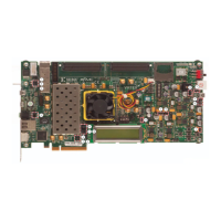
Illustrates the VCU128 evaluation board's hardware components and their interconnections.
Lists the key hardware features and capabilities of the VCU128 evaluation board.
Details the physical dimensions, environmental operating conditions, and voltage requirements.
Provides essential safety guidelines to prevent ESD damage to electronic components.
Guides users to identify the physical location of board components using figures.
Explains the physical installation process of the VCU128 board into a PC chassis.
Describes the methods and modes for configuring the FPGA on the VCU128 board.
Lists the voltage levels supplied to the FPGA's I/O banks.
Describes the 4.5 GB DDR4 memory system, its specifications, and FPGA connections.
Details the 288 MB RLD3 memory system, its specifications, and FPGA connections.
Describes the QDR4 SRAM component, its specifications, and FPGA connections.
Explains the Quad SPI flash memory used for boot images and data storage.
Covers JTAG connectivity for configuration and debugging via USB.
Lists and details the various clock sources available for the FPGA.
Explains the high-speed serial transceivers and their organization.
Details the PCIe interface, its speeds, and connectivity.
Describes the QSFP28 connectors for high-speed optical modules.
Explains the Ethernet PHY for network connectivity.
Details the I2C bus implementation, including switches and topology.
Defines the board's status and user LEDs, indicating operational states.
Covers user-programmable general-purpose I/O including LEDs and switches.
Describes the onboard power switch and configuration pushbutton.
Explains the FMC+ connector and its implementation on the board.
Provides an overview of the board's power supply architecture.
Details the onboard Zynq system controller and its management utility.
Outlines the supported FPGA configuration modes and settings.
Introduces the pinout details for the FMC connector J18 based on VITA 57.4.
Explains the purpose and usage of the Xilinx Design Constraints (XDC) file template.
Introduces the EU directives and standards the product conforms to.
Lists relevant European Union directives for safety and compatibility.
Details EMC standards related to IT equipment disturbance and immunity.
Explains WEEE, RoHS, and CE compliance markings and their significance.
Points to Xilinx support resources like Answers, Documentation, and Forums.
Describes tools for accessing Xilinx documents, videos, and tutorials.
Lists relevant documents, datasheets, and websites for further information.
Contains crucial legal disclaimers, warranties, and terms of use.
| Memory | DDR4 |
|---|---|
| Memory Capacity | 16 GB |
| PCIe | Gen3 x16 |
| Power Supply | 12V |
| LED Indicators | Yes |
| USB | USB 3.0 |
| FPGA Device | Virtex UltraScale+ VU9P |
| Connectivity | PCIe |
| Ethernet | 10 GbE |

