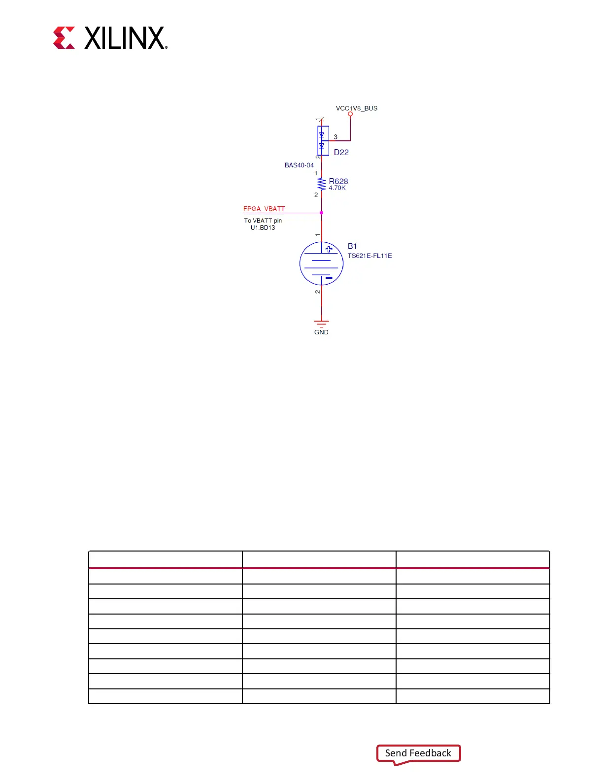
Figure 6: Encryption Key Backup Circuit
X21956-112918
The Seiko TS621E rechargeable 1.5V lithium buon-type baery B1 is soldered to the board
with the posive output connected to the XCVU37P device U1 VBATT pin BD13. The baery
supply current IBATT specicaon is 150 nA maximum when the board power is o. B1 is
charged from the VCC1V8_BUS 1.8V rail through a series diode with a typical forward voltage
drop of 0.38V and 4.7 KΩ current limit resistor. The nominal charging voltage is 1.42V.
I/O Voltage Rails
There are 12 I/O banks and 2 high-bandwidth memory (HBM) banks available on the XCVU37P
device. The VCU128 board does not use the HBM banks. The voltages applied to the FPGA I/O
banks on the VCU128 board are listed in the following table.
Table 5: I/O Bank Voltage Rails
FPGA (U1) Bank Power Supply Rail Net Name Voltage
Bank 0 VCC1V8 1.8V
HP bank 64 DDR4_VDDQ_1V2 1.2V
HP bank 65 DDR4_VDDQ_1V2 1.2V
HP bank 66 DDR4_VDDQ_1V2 1.2V
HP bank 67 VCC1V8 1.8V
HP bank 68 QDR4_VDDQ_1V2 1.2V
HP bank 69 QDR4_VDDQ_1V2 1.2V
HP bank 70 QDR4_VDDQ_1V2 1.2V
HP bank 71 VADJ 1.8V
Chapter 3: Board Component Descriptions
UG1302 (v1.0) December 21, 2018 www.xilinx.com
VCU128 Board User Guide 19