Do you have a question about the Xilinx VC709 and is the answer not in the manual?
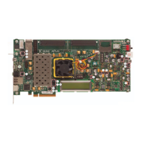
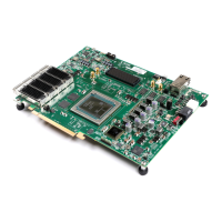
Provides an overview of the VC709 board and lists its key components and features.
Detailed descriptions of the components located on the VC709 board.
Explains the various clock sources and their distribution on the board.
Details the GTH transceivers, their banks, and connectivity to other interfaces.
Describes the PCI Express edge connector and SFP/SFP+ module interfaces.
Covers USB-to-UART bridge and I2C bus functionality for communication.
Details status LEDs, user LEDs, pushbuttons, and DIP switches.
Explains power switches, configuration switches, and the overall power system.
Describes the FMC connector and XADC for analog measurements.
Details FPGA configuration methods, mode switches, and boot settings.
Lists the default settings for the GPIO DIP switch SW2.
Details the default settings for the configuration DIP switch SW11.
Provides default positions for various jumpers on the board.
Shows the pinout diagram for the FMC1 HPC connector (J35).
Lists the user constraints file (UCF) pin assignments for the VC709 board.
| Brand | Xilinx |
|---|---|
| Model | VC709 |
| Category | Motherboard |
| Language | English |
