8 www.xilinx.com VC709 Evaluation Board
UG887 (v1.0) February 4, 2013
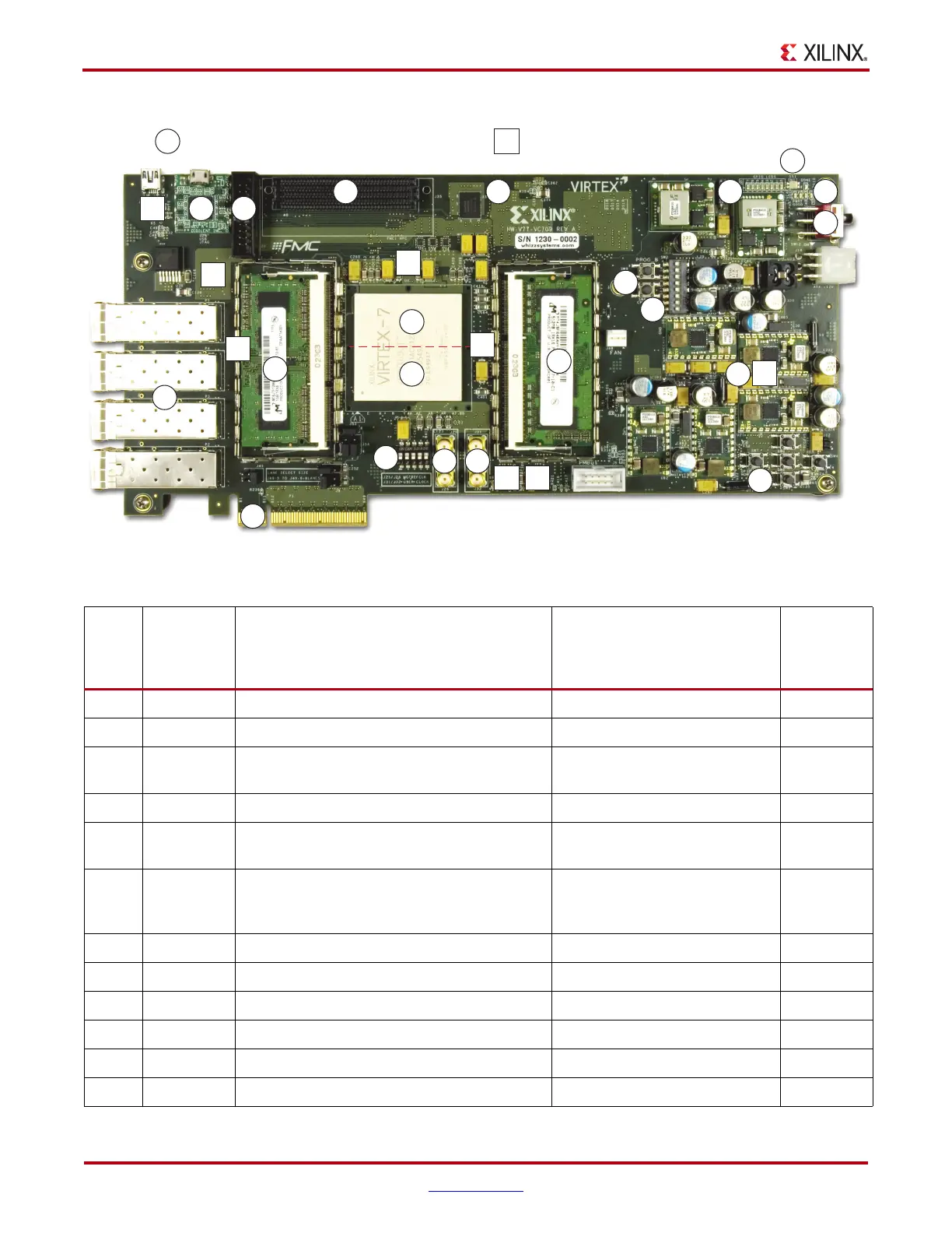
Chapter 1: VC709 Evaluation Board Features
X-Ref Target - Figure 1-2
Figure 1-2: VC709 Board Component Locations
00
Round callout references a component
on the front side of the board.
00
Square callout references a component
on the back side of the board.
4
2
12
11
1
UG887_c1_02_082612
2
19
18
26
17
10
20
8 7
23
22 3 16 25
21
24
13
15
5
6
27
9 14
26
Table 1-1: VC709 Board Component Descriptions
Callout
Reference
Designator
Component Description Notes
Schematic
0381499
Page
Number
1
U1 Virtex-7 FPGA XC7VX690T-2FFG1761CES
2
J1, J3 Two DDR3 SODIMM memories (4 GB each) Micron MT8KTF51264HZ-1G9E1 10, 14
3
U3 BPI parallel NOR flash memory (1 Gb)
Micron/Numonyx
PC28F00AG18FE
24
4
U26 USB JTAG interface (micro-B USB connector) Digilent USB JTAG module 5
5
U51
System clock, 200 MHz, LVDS (back side of
board)
SiTime
SIT9102-243N25E200.0000
3
6
U34
I
2
C programmable user clock LVDS,
156.250 MHz default frequency (back side of
board)
Silicon Labs
SI570BAB0000544DG (I²C 0x5D)
3
7
J31, J32 User SMA clock Rosenberger 32K10K-400L5 3
8
J25, J26 GTH transceiver SMA reference clock Rosenberger 32K10K-400L5 30
9
U24 Jitter-attenuated clock (back side of board) Silicon Labs SI5324C-C-GM 4
10
U1 GTH transceiver Quad 111–Quad 119 Embedded within FPGA U1 30, 36–38
11
P1 PCI Express connector 8-lane card edge connector 35
12
P2–P5 4 X SFP/SFP+ module connector (I²C 0x50) Molex 74441-0010 31–35