EasyManuals Logo

Xilinx VC709 User Manual

Xilinx VC709
96 pages
To Next Page IconTo Next Page
To Previous Page IconTo Previous Page
Page #24 background imageLoading...
Page #24 background image
24 www.xilinx.com VC709 Evaluation Board
UG887 (v1.0) February 4, 2013
Chapter 1: VC709 Evaluation Board Features
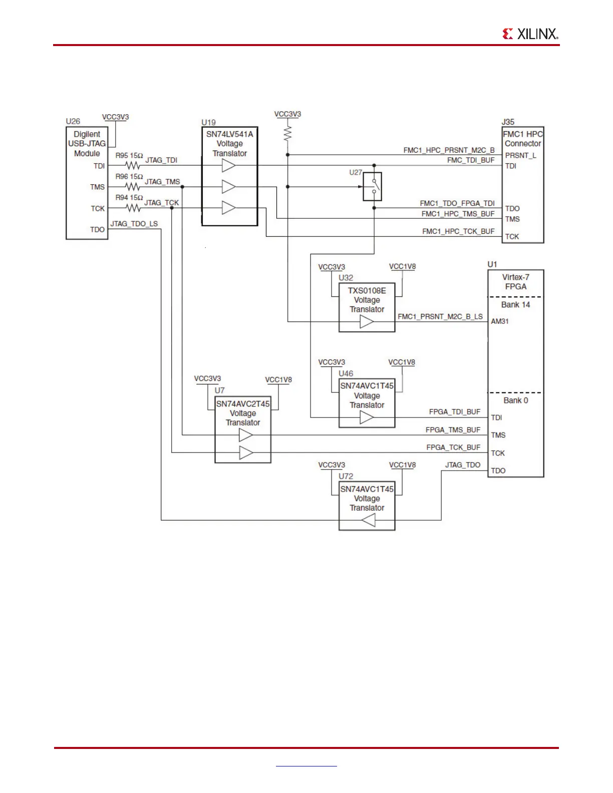
The JTAG circuit details are shown in Figure 1-6.
Clock Generation
The VC709 board provides six clock sources for the FPGA. Table 1-7 lists the source devices
for each clock.
X-Ref Target - Figure 1-6
Figure 1-6: JTAG Circuit
UG855_c1_06_011013

Other manuals for Xilinx VC709

Questions and Answers:

Question and Answer IconNeed help?

Do you have a question about the Xilinx VC709 and is the answer not in the manual?

Xilinx VC709 Specifications

General IconGeneral
BrandXilinx
ModelVC709
CategoryMotherboard
LanguageEnglish

Related product manuals