VC709 Evaluation Board www.xilinx.com 61
UG887 (v1.0) February 4, 2013
Configuration Options
Table 1-25 describes the XADC header J19 pin functions.
Configuration Options
The FPGA on the VC709 board can be configured by the following methods:
• Master BPI (uses the linear BPI flash).
• JTAG (Digilent USB-to-JTAG Bridge only). See USB JTAG, page 23 for more
information.
See 7 Series FPGAs Configuration User Guide (UG470
) for further details on configuration
modes.
The method used to configure the FPGA is controlled by the mode pin (M2, M1, M0)
settings selected through DIP switch SW11. Table 1-26 lists the supported mode switch
settings.
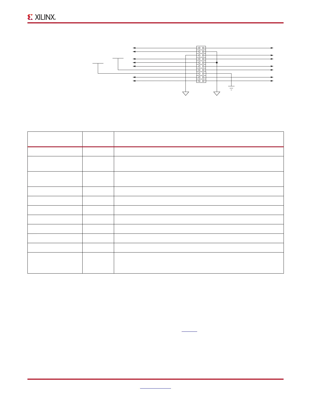
X-Ref Target - Figure 1-26
Figure 1-26: XADC header (J19)
UG887_c1_26_090612
XADC_VP
XADC_VAUX0N
XADC_VAUX8P
XADC_DXN
XADC_VCC_HEADER
XADC_VN
XADC_VAUX0P
XADC_VAUX8N
XADC_DXP
XADC_VREF
XADC_GPIO_0
XADC_GPIO_2
XADC_GPIO_1
XADC_GPIO_3
J19
1
3
5
7
9
11
13
15
17
19
2
4
6
8
10
12
14
16
18
20
GND
XADC_AGNDXADC_AGND
XADC_VCC5V0
VADJ
Table 1-25: XADC Header J19 Pinout
Net Name
J19 Pin
Number
Description
VN, VP 1, 2 Dedicated analog input channel for the XADC.
XADC_VAUX0P, N 3, 6
Auxiliary analog input channel 0. Also supports use as I/O inputs when
anti-alias capacitor is not present.
XADC_VAUX8N, P 7, 8
Auxiliary analog input channel 8. Also supports use as I/O inputs when
anti-alias capacitor is not present.
DXP, DXN 9, 12 Access to thermal diode.
XADC_AGND 4, 5, 10 Analog ground reference.
XADC_VREF 11 1.25V reference from the board.
XADC_VCC5V0 13 Filtered 5V supply from board.
XADC_VCC_HEADER 14 Analog 1.8V supply for XADC.
VA DJ 1 5 V
CCO
supply for bank which is the source of DIO pins.
GND 16 Digital ground (board) reference
XADC_GPIO_3, 2, 1, 0 19, 20, 17, 18
Digital I/O. These pins should come from bank 15. These I/Os should not be
shared with other functions because they are required to support 3-state
operation.