VC709 Evaluation Board www.xilinx.com 19
UG887 (v1.0) February 4, 2013
Feature Descriptions
The VC709 DDR3 SODIMM interfaces adhere to the constraints guidelines documented in
the DDR3 Design Guidelines section of 7 Series FPGAs Memory Interface Solutions
User Guide (UG586
). The VC709 DDR3 SODIMM interfaces are 40Ω impedance
implementations. Other memory interface details are available in UG586
and
7 Series FPGAs Memory Resources User Guide (UG473
).
Linear BPI Flash Memory
[Figure 1-2, callout 3]
The linear BPI flash memory located at U3 provides 128 MB of nonvolatile storage that can
be used for configuration or software storage. The data, address, and control signals are
connected to the FPGA. The BPI flash memory device is packaged in a 64-pin BGA.
• Part number: PC28F00AG18FE (Numonyx)
• Supply voltage: 1.8V
• Datapath width: 16 bits (26 address lines and 7 control signals)
• Data rate: Up to 40 MHz
The linear BPI flash memory can synchronously configure the FPGA in Master BPI mode at
the 40 MHz data rate supported by the PC28F00AG18FE flash memory by using a
configuration bitstream generated with BitGen options for synchronous configuration and
for configuration clock division. The fastest configuration method uses the external
80 MHz oscillator connected to the FPGA's EMCCLK pin with a bitstream that has been
built to divide the configuration clock by two. The division is necessary to remain within
the synchronous read timing specifications of the flash memory.
Multiple bitstreams can be stored in the linear BPI flash. The two most significant address
bits (A25, A24) of the flash memory are connected to DIP switch SW11 positions 1 and 2
respectively, and to the RS1 and RS0 pins of the FPGA. By placing valid XC7VX690T
bitstreams at four different offset addresses in the flash memory, 1 of the 4 bitstreams can
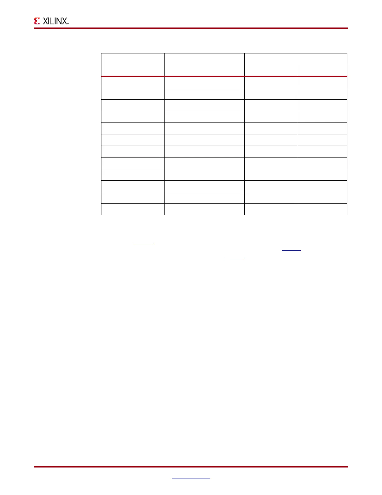
AU18 DDR3_B_CLK1_P 104 CK1_N
AW17 DDR3_B_CKE0 73 CKE0
AW18 DDR3_B_CKE1 74 CKE1
AV19 DDR3_B_RAS_B 110 RAS_B
AU19 DDR3_B_WE_B 113 WE_B
AT20 DDR3_B_CAS_B 115 CAS_B
AT16 DDR3_B_ODT0 116 ODT0
AW16 DDR3_B_ODT1 120 ODT1
AV16 DDR3_B_S0_B 114 S0_B
AT19 DDR3_B_S1_B 121 S1_B
BB19 DDR3_B_RESET_B 30 RESET_B
AU16 DDR3_B_TEMP_EVENT_B 198 EVENT_B
Table 1-5: DDR3 SODIMM Socket J3 Connections to the FPGA (Cont’d)
XCVX690T (U1) Pin Net Name
SODIMM Memory J3
Pin Number Pin Name