VC709 Evaluation Board www.xilinx.com 49
UG887 (v1.0) February 4, 2013
Feature Descriptions
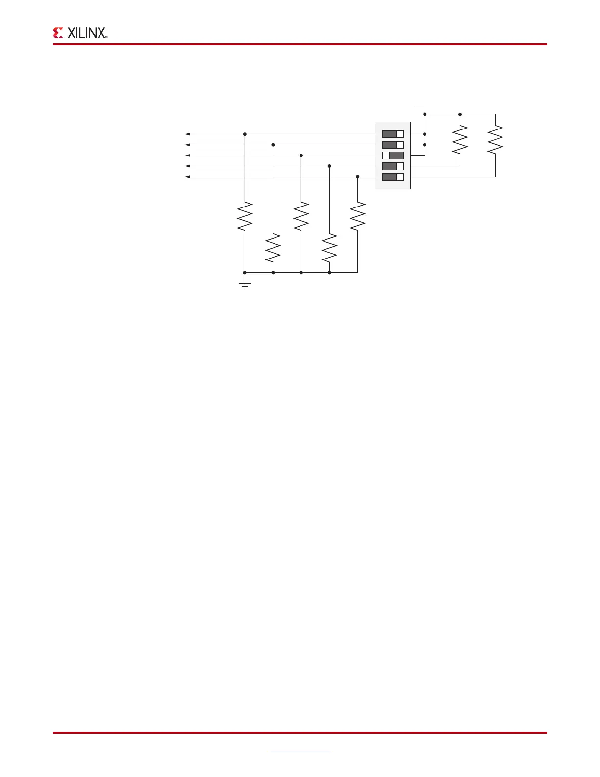
Figure 1-23 shows the SW11 circuit.
VITA 57.1 FMC1 HPC Connector (Partially Populated)
[Figure 1-2, callout 22]
The VC709 board implements one instance of the FMC HPC VITA 57.1 specification
connector. This section discusses the FMC1 HPC J35 connector.
Note:
The FMC1 HPC J35 connector is a keyed connector oriented so that a plug-on card faces
away from the VC709 board.
The VITA 57.1 FMC standard calls a high pin count (HPC), 400 pin 10 x 40 position form
factor connector. The 10 x 40 rows of an FMC HPC connector provides pins for up to:
• 160 single-ended or 80 differential user-defined signals
• 10 GTH transceivers
•2 GTH clocks
•4 differential clocks
• 159 ground and 15 power connections
The VC709 board FMC1 HPC connector J35 implements a subset of the maximum signal
and clock connectivity capabilities:
• 80 differential user-defined pairs:
• 34 LA pairs (LA00-LA33)
• 24 HA pairs (HA00-HA23)
• 22 HB pairs (HB00-HB21)
• 10 GTH transceivers
•2 GTH clocks
•2 differential clocks
The FMC1 HPC signals are distributed across GTH Quads 117, 118, and 119.
X-Ref Target - Figure 1-23
Figure 1-23: Configuration Mode and Upper Linear Flash Address Switch
UG887_c1_23_090612
SDA05H1SBD
SW11
R226
220Ω
0.1 W
1%
R227
220Ω
0.1 W
1%
VCC1V8
FPGA_M2
FPGA_M1
FPGA_M0
FLASH_A25
FLASH_A24
R341
1.21kΩ
0.1 W
1%
R340
1.21kΩ
0.1 W
1%
R339
1.21kΩ
0.1 W
1%
R338
1.21kΩ
0.1 W
1%
R337
1.21kΩ
0.1 W
1%
1
2
3
4
5
10
9
8
7
6
GND