VC709 Evaluation Board www.xilinx.com 23
UG887 (v1.0) February 4, 2013
Feature Descriptions
USB JTAG
[Figure 1-2, callout 4]
JTAG configuration is provided solely through a Digilent onboard USB-to-JTAG
configuration logic module (U26) where a host computer accesses the VC709 board JTAG
chain through a type-A (host side) to micro-B (VC709 board side) USB cable.
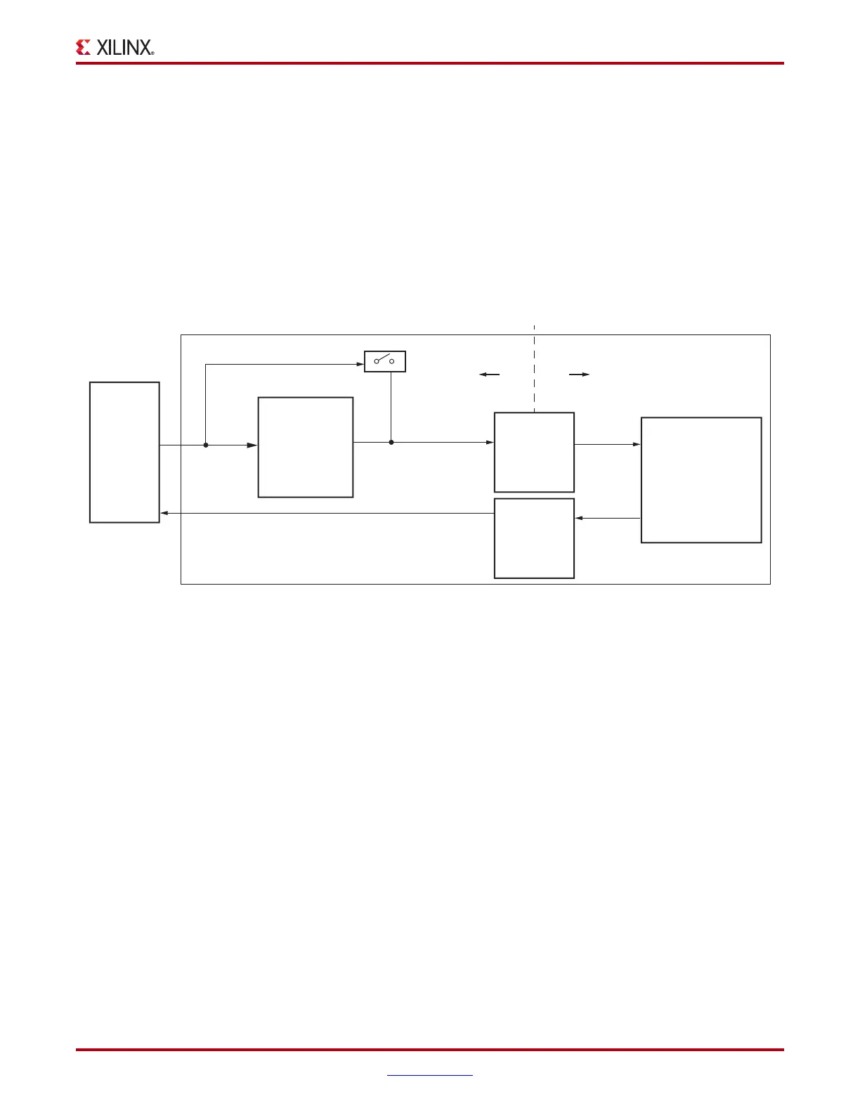
The JTAG chain of the VC709 board is illustrated in Figure 1-5. JTAG configuration is
allowed at any time regardless of FPGA mode pin settings. JTAG initiated configuration
takes priority over the configuration method selected through the FPGA mode pin settings
at SW11.
When an FMC mezzanine card is attached to the VC709 HPC connector J35, it is
automatically added to the JTAG chain through electronically controlled single-pole
single-throw (SPST) switch U27. The SPST switch is in a normally closed state and
transitions to an open state when an FMC mezzanine card is attached. Switch U27 adds an
attached FMC mezzanine card to the FPGAs JTAG chain as determined by the
FMC_HPC_PRSNT_M2C_B signal. The attached FMC card must implement a
TDI-to-TDO connection via a device or bypass jumper for the JTAG chain to be completed
to the FPGA U1.
The JTAG connectivity on the VC709 board allows a host computer to download
bitstreams to the FPGA using the Xilinx® iMPACT software. In addition, the JTAG
connector allows debug tools such as the ChipScope™ Pro analyzer or a software
debugger to access the FPGA. The iMPACT software tool can also indirectly program the
linear BPI flash memory. To accomplish this, the iMPACT software configures the FPGA
with a temporary design to access and program the BPI memory device.
X-Ref Target - Figure 1-5
Figure 1-5: JTAG Chain Block Diagram
UG887_c1_05_100912
1.8V3.3V
TDI TDO
USB
Module
U1
FPGA
TDI
TDO
JTAG Chain
FMC HPC1
Voltage
Translator
Voltage
Translator