VC709 Evaluation Board www.xilinx.com 7
UG887 (v1.0) February 4, 2013
Feature Descriptions
Feature Descriptions
Figure 1-2 shows the VC709 board. Each numbered feature that is referenced in Figure 1-2
is described in Table 1-1 and following sections.
Note:
The image in Figure 1-2 is for reference only and might not reflect the current revision of the
board.
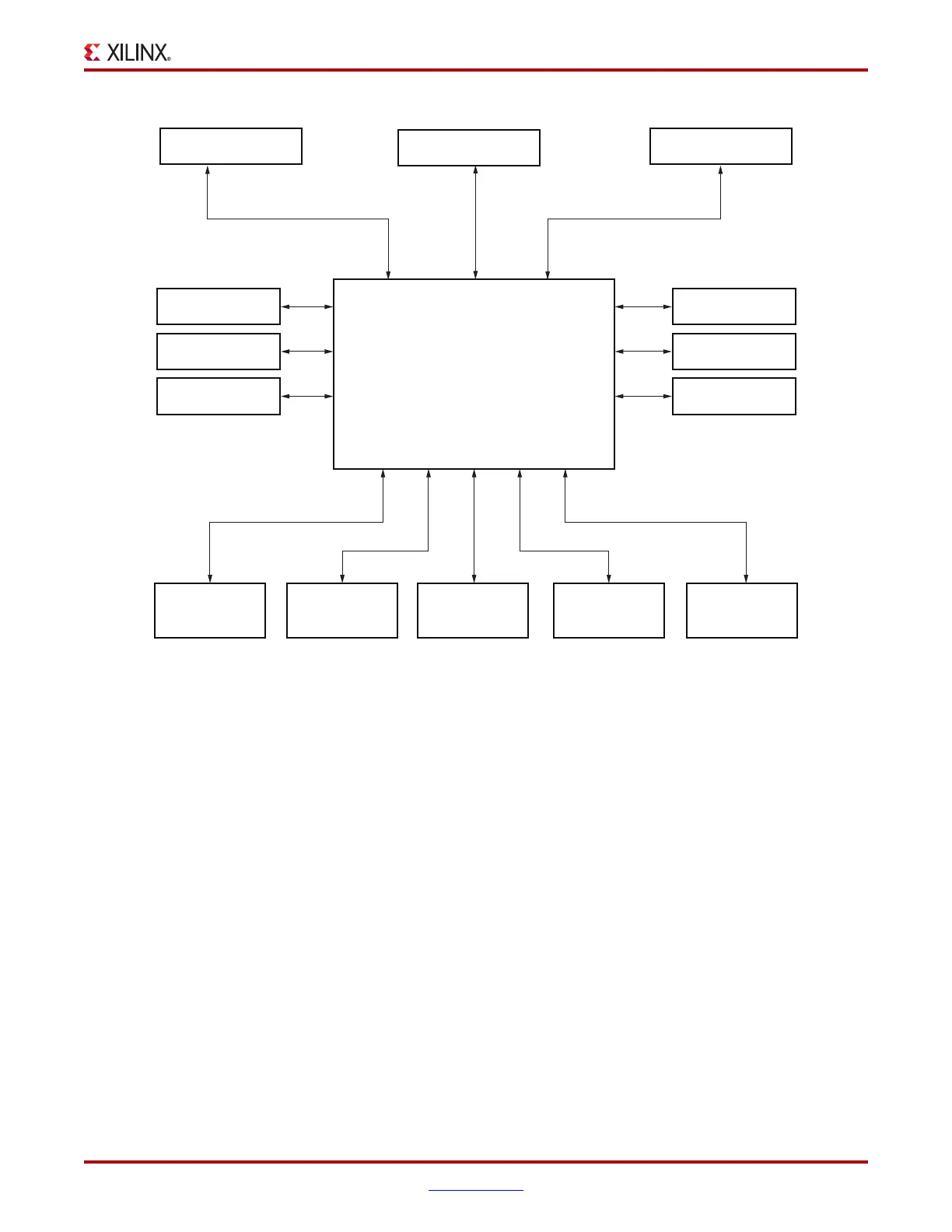
X-Ref Target - Figure 1-1
Figure 1-1: VC709 Board Block Diagram
HPC FMC Connector
4 GB DDR3 Memory
(SODIMM)
1 KB EEPROM
(I
2
C)
I
2
C Bus Switch
DIP Switch SW11
Config and
Flash Addr
USB-to-UART
Bridge
JTAG Interface
Micro-B USB
Connector
4X SFP+ Cage
UG887_c1_01_012113
8-lane PCI Express
Edge Connector
SI5324C
Clock Recovery
128 MB Linear BPI
Flash Memory
Virtex-7 FPGA
XC7VX690T-2FFG1761C
User Switches,
Buttons, and LEDs
XADC Header
Differential Clock
GTH SMA Clock
4 GB DDR3 Memory
(SODIMM)