66 www.xilinx.com VC709 Evaluation Board
UG887 (v1.0) February 4, 2013
Appendix A: Default Switch and Jumper Settings
Configuration DIP Switch SW11
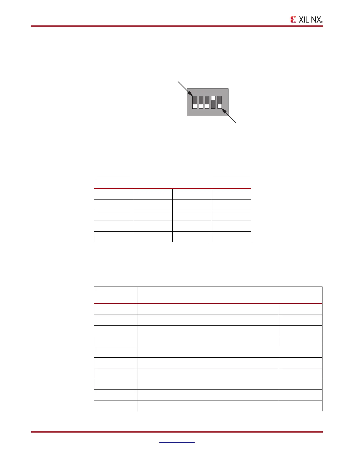
See Figure 1-2, page 8 Item 29 for the location of SW11. Default settings are shown in
Figure A-2 and details are listed in Table A-2.
The default mode setting M[2:0] = 010 selects Master BPI configuration at board
power-on.
Default Jumper Settings
See Figure 1-2, page 8 for locations of jumpers listed in Table A-3.
X-Ref Target - Figure A-2
Figure A-2: SW11 Default Settings
Tab le A- 2 : SW11 Default Switch Settings
Position Function Default
1 FLASH_A25 A25 Off
2 FLASH_A24 A24 Off
3FPGA_M2 M0 Off
4FPGA_M1 M1 On
5FPGA_M0 M3 Off
UG887_aA_02_083012
1
OFF Position = 0
ON Position = 1
2 3 4 5
A25
A24
M2
M1
M0
Tab le A- 3 : Default Jumper Settings
Jumper Function
Default Jumper
Position
J9 XADC GND ferrite filter bypass jumper None
J10 XADC GND-to-XADC_AGND jumper 1-2
J42 XADC external 1.2V or internal VREFP selector 1-2
J43 XADC VCC select header 2-3
J53 XADC VCC5V0-to-XADC_VCC5V0 jumper 1-2
J54 XADC REF3012 U35 VIN select 1-2
J49 PCIe bus width select header 1-2
J11 TI controller U42 Addr 52 Reset jumper None
J12 TI controller U43 Addr 53 Reset jumper None
J50 TI controller U64 Addr 54 Reset jumper None