30 www.xilinx.com VC709 Evaluation Board
UG887 (v1.0) February 4, 2013
Chapter 1: VC709 Evaluation Board Features
One possible I/O standard for the FPGA design clock input is:
NET "sysclk_233_p" LOC = "AY18" | IOSTANDARD = DIFF_SSTL15_DCI | #Bank
32 MRCC input
NET "sysclk_233_n" LOC = "AY17" | IOSTANDARD = DIFF_SSTL15_DCI | #Diff.
Rterm R43 DNP
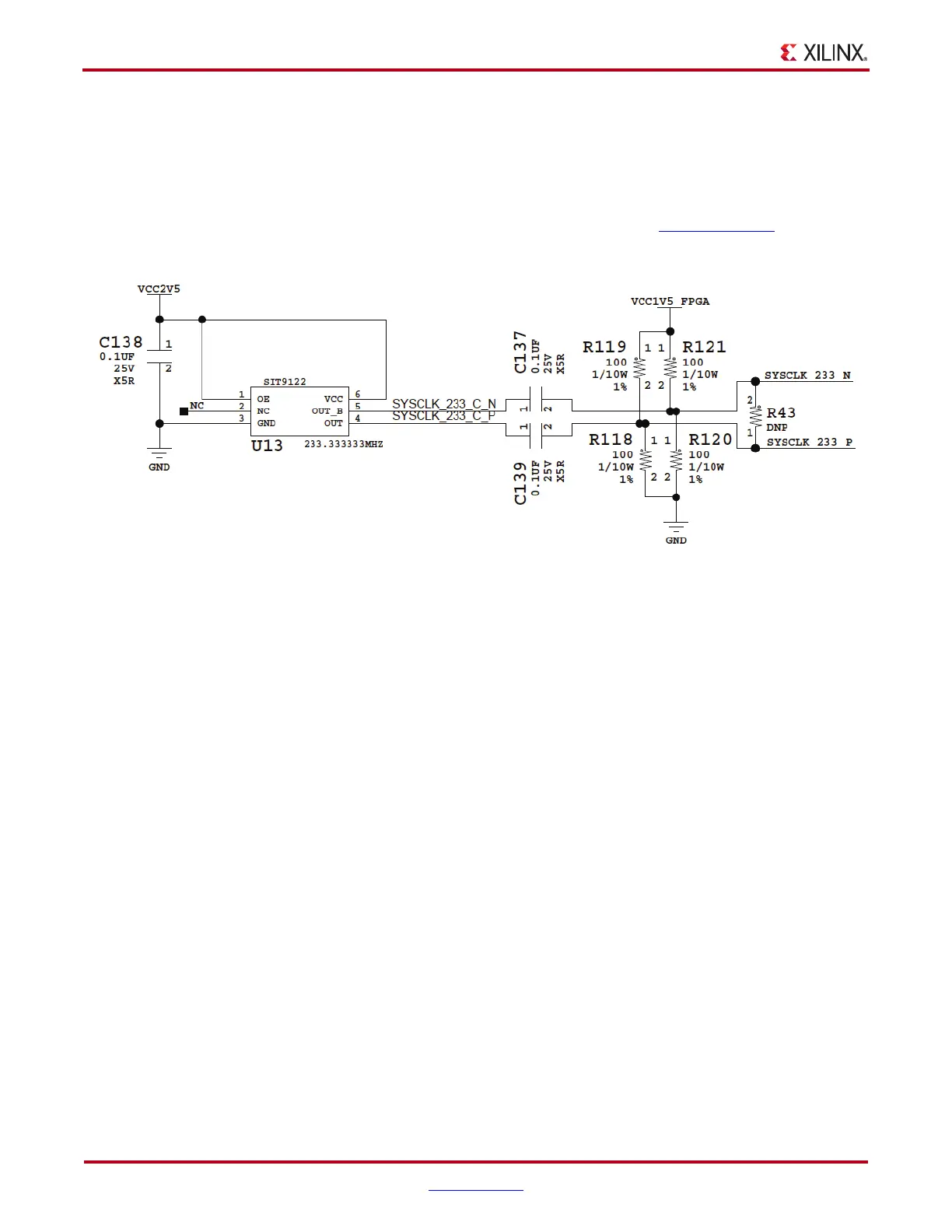
For more details, see the Si Time SiT9122 data sheet (SiTime www.sitime.com). The system
clock circuit is shown in Figure 1-12.
GTH Transceivers
[Figure 1-2, callout 10]
The VC709 board provides access to 22 GTH transceivers:
• Eight of the GTH transceivers are wired to the PCI Express x8 endpoint edge
connector (P1) fingers.
• Ten of the GTH transceivers are wired to the FMC HPC connector (J35).
• Four of the GTH transceivers are wired to the four SFP/SFP+ connectors (P2, P3, P4,
P5).
The GTH transceivers in 7 series FPGAs are grouped into four channels described as
Quads. The reference clock for a Quad can be sourced from the Quad above or Quad below
the GTH Quad of interest. There are six GTH Quads on the VC709 board with connectivity
as shown here:
•Quad 113:
• MGTREFCLK0 - Si5324 jitter attenuator
• MGTREFCLK1 - SMA clock
• Contains 4 GTH transceivers with one each allocated to SFP 1 through 4
•Quad 114:
• MGTREFCLK0 - No clock
• MGTREFCLK1 - No clock
X-Ref Target - Figure 1-12
Figure 1-12: Memory Clock Source
UG887_c1_12_011013