VC709 Evaluation Board www.xilinx.com 9
UG887 (v1.0) February 4, 2013
Feature Descriptions
Virtex-7 XC7VX690T-2FFG1761CES FPGA
[Figure 1-2, callout 1]
The VC709 board is populated with the Virtex-7 XC7VX690T-2FFG1761CES FPGA.
For further information on Virtex-7 FPGAs, see 7 Series FPGAs Overview (DS180
).
FPGA Configuration
The VC709 board supports two of the five 7 series FPGA configuration modes:
• Master BPI using the onboard linear BPI flash memory
• JTAG using a type-A to micro-B USB cable for connecting the host PC to the VC709
board configuration port
Each configuration interface corresponds to one or more configuration modes and bus
widths as listed in Table 1-2. The mode switches M2, M1, and M0 are on SW11 positions 3,
4, and 5 respectively as shown in Figure 1-3.
Note:
To determine the FPGA device type resident on the VC709 board, refer to the Master Answer
Record listed in Appendix F, Additional Resources.
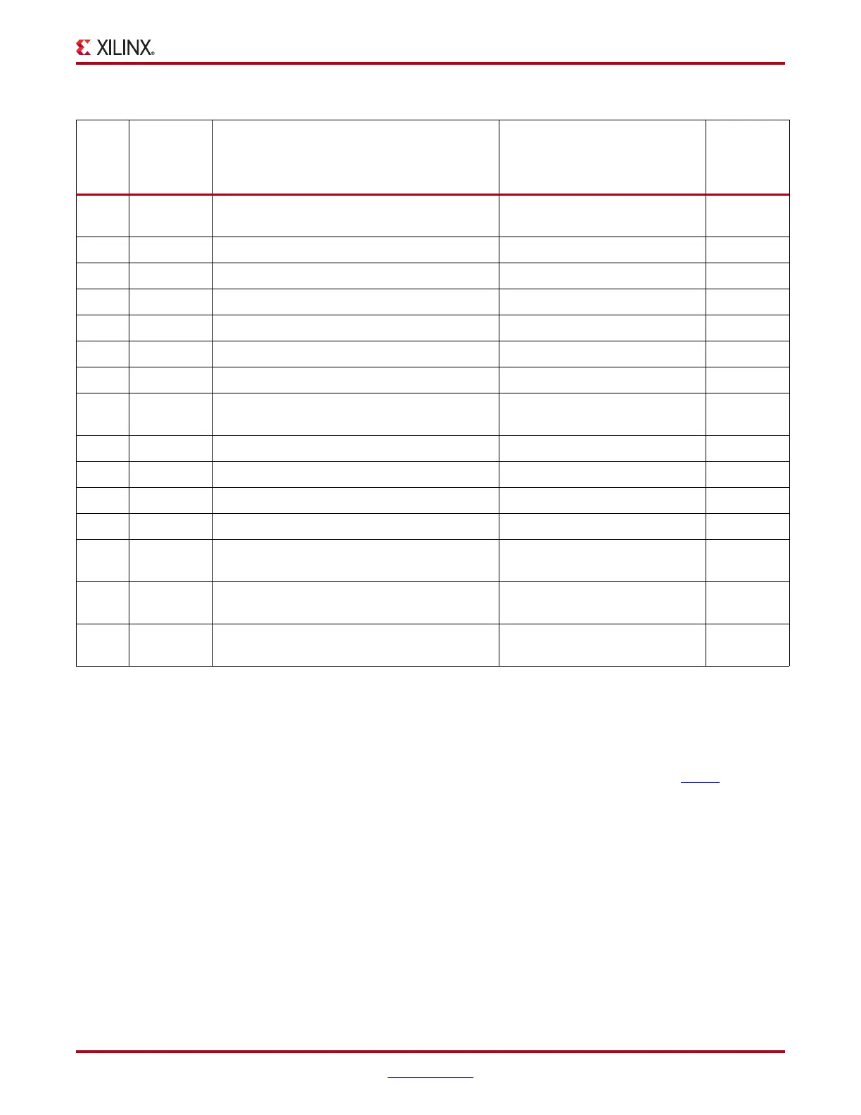
13
U44, J17
USB-to-UART bridge with mini-B USB
connector
Silicon Labs CP2103GM 6
14
U52 I
2
C bus switch (I²C 0x74) (back side of board) TI PCA9548ARGER 29
15
U14 I
2
C bus switch (I²C 0x75) (back side of board) TI PCA9546ARGVR 29
16
DS2–DS9 User LEDs, Green Lumex SML-LX0603GW 25
17
SW3–SW7 User pushbuttons, active-High E-Switch TL3301EP100QG 25
18
SW2 User DIP switch, active-High 8-pole C and K SDA08H1SBD 25
19
SW8, SW9 CPU RESET, FPGA PROG pushbuttons E-Switch TL3301EP100QG 25, 7
20
SW11
Configuration mode/upper linear flash
address DIP switch
5-pole C and K SDA05H1IBD 7
21
SW12 Power on/off slide switch C and K 1201M2S3AQE2 46
22
J35 FMC HPC connector Samtec ASP_134486_01 18–21
23
J19 Xilinx XADC header 2 x 10 0.1-inch male header 27
24
DS1 INIT LED, dual color Red/Green Avago HSMF-C155 38
25
DS10, DS14,
DS16–DS18
Power ON and Power GOOD LEDs Lumex SML-LX0603GW 38
26
Various
Power management system (front and back
side of board)
TI UCD9248PFC in conjunction
with various regulators
45–56
27
U13
Memory clock, 233.33 MHz, LVDS (back side
of board)
SiTime
SIT9122AC-2D3-25E233.333333
3
Table 1-1: VC709 Board Component Descriptions (Cont’d)
Callout
Reference
Designator
Component Description Notes
Schematic
0381499
Page
Number