VC709 Evaluation Board www.xilinx.com 11
UG887 (v1.0) February 4, 2013
Feature Descriptions
Dual DDR3 Memory SODIMMs
[Figure 1-2, callout 2]
The memory modules at J1 and J3 are 4 GB DDR3 small outline dual-inline memory
module (SODIMMs), providing volatile synchronous dynamic random access memory
(SDRAM) for storing user code and data.
• Part number: MT8KTF51264HZ-1G9E1 (Micron Technology)
• Supply voltage: 1.5V
• Datapath width: 64 bits
• Data rate: Up to 1,866 MT/s
Each DDR3 interface is implemented across three I/O banks: 37, 38, and 39 for J1 and 31, 32
and 33 for J3. Each bank is a 1.5V high-performance bank having a dedicated DCI VRP/N
resistor connection. An external 0.75V reference V
TTREF
is provided for data interface
banks 37, 39, 31, and 33. Any interface connected to these banks that requires a reference
voltage must use this FPGA voltage reference. The connections between the DDR3
memory SODIMM sockets and the FPGA are listed in Table 1-4 and Table 1-5.
Bank 35 VADJ_FPGA 1.8V
Bank 36 FMC1_VIO_B_M2C Variable
Bank 37 VCC1V5_FPGA 1.5V
Bank 38 VCC1V5_FPGA 1.5V
Bank 39 VCC1V5_FPGA 1.5V
Table 1-3: I/O Voltage Rails (Cont’d)
FPGA (U1) Bank Power Supply Rail Net Name Voltage
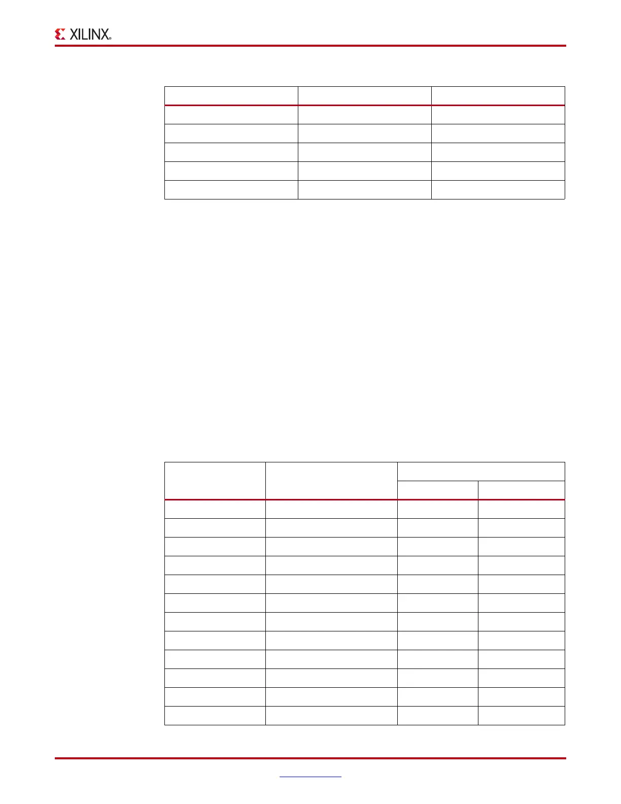
Table 1-4: DDR3 SODIMM Socket J1 Connections to the FPGA
XCVX690T (U1) Pin Net Name
SODIMM Memory J3
Pin Number Pin Number
A20 DDR3_A_A0 98 A0
B19 DDR3_A_A1 97 A1
C20 DDR3_A_A2 96 A2
A19 DDR3_A_A3 95 A3
A17 DDR3_A_A4 92 A4
A16 DDR3_A_A5 91 A5
D20 DDR3_A_A6 90 A6
C18 DDR3_A_A7 86 A7
D17 DDR3_A_A8 89 A8
C19 DDR3_A_A9 85 A9
B21 DDR3_A_A10 107 A10/AP
B17 DDR3_A_A11 84 A11