VC709 Evaluation Board www.xilinx.com 15
UG887 (v1.0) February 4, 2013
Feature Descriptions
E19 DDR3_A_CLK0_P 101 CK0_P
F19 DDR3_A_CLK1_N 104 CK1_N
G19 DDR3_A_CLK1_P 102 CK1_P
K19 DDR3_A_CKE0 73 CKE0
J18 DDR3_A_CKE1 74 CKE1
E20 DDR3_A_RAS_B 110 RAS_B
F20 DDR3_A_WE_B 113 WE_B
K17 DDR3_A_CAS_B 115 CAS_B
H20 DDR3_A_ODT0 116 ODT0
H18 DDR3_A_ODT1 120 ODT1
J17 DDR3_A_S0_B 114 S0_B
J20 DDR3_A_S1_B 121 S1_B
P18 DDR3_A_RESET_B 30 RESET_B
G17 DDR3_A_TEMP_EVENT_B 198 EVENT_B
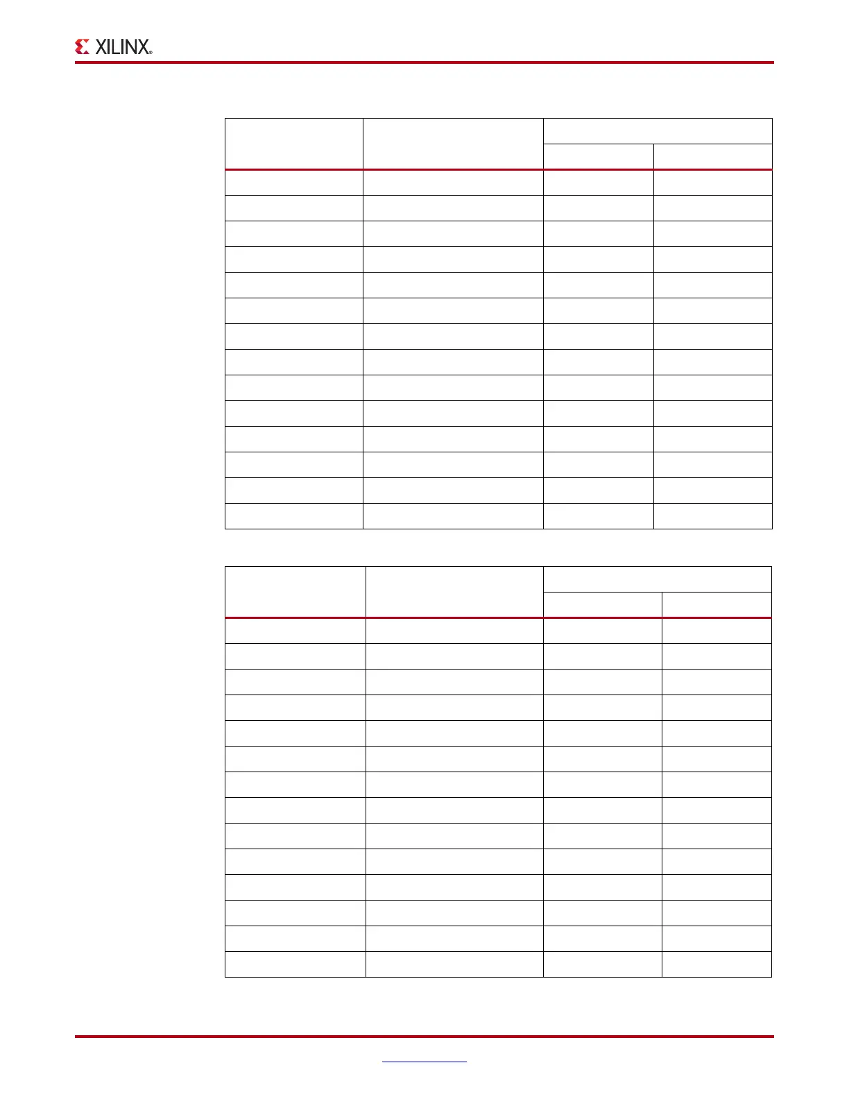
Table 1-5: DDR3 SODIMM Socket J3 Connections to the FPGA
XCVX690T (U1) Pin Net Name
SODIMM Memory J3
Pin Number Pin Name
AN19 DDR3_B_A0 98 A0
AR19 DDR3_B_A1 97 A1
AP20 DDR3_B_A2 96 A2
AP17 DDR3_B_A3 95 A3
AP18 DDR3_B_A4 92 A4
AJ18 DDR3_B_A5 91 A5
AN16 DDR3_B_A6 90 A6
AM16 DDR3_B_A7 86 A7
AK18 DDR3_B_A8 89 A8
AK19 DDR3_B_A9 85 A9
AM17 DDR3_B_A10 107 A10/AP
AM18 DDR3_B_A11 84 A11
AL17 DDR3_B_A12 83 A12_BC_N
AK17 DDR3_B_A13 119 A13
Table 1-4: DDR3 SODIMM Socket J1 Connections to the FPGA (Cont’d)
XCVX690T (U1) Pin Net Name
SODIMM Memory J3
Pin Number Pin Number