48 www.xilinx.com VC709 Evaluation Board
UG887 (v1.0) February 4, 2013
Chapter 1: VC709 Evaluation Board Features
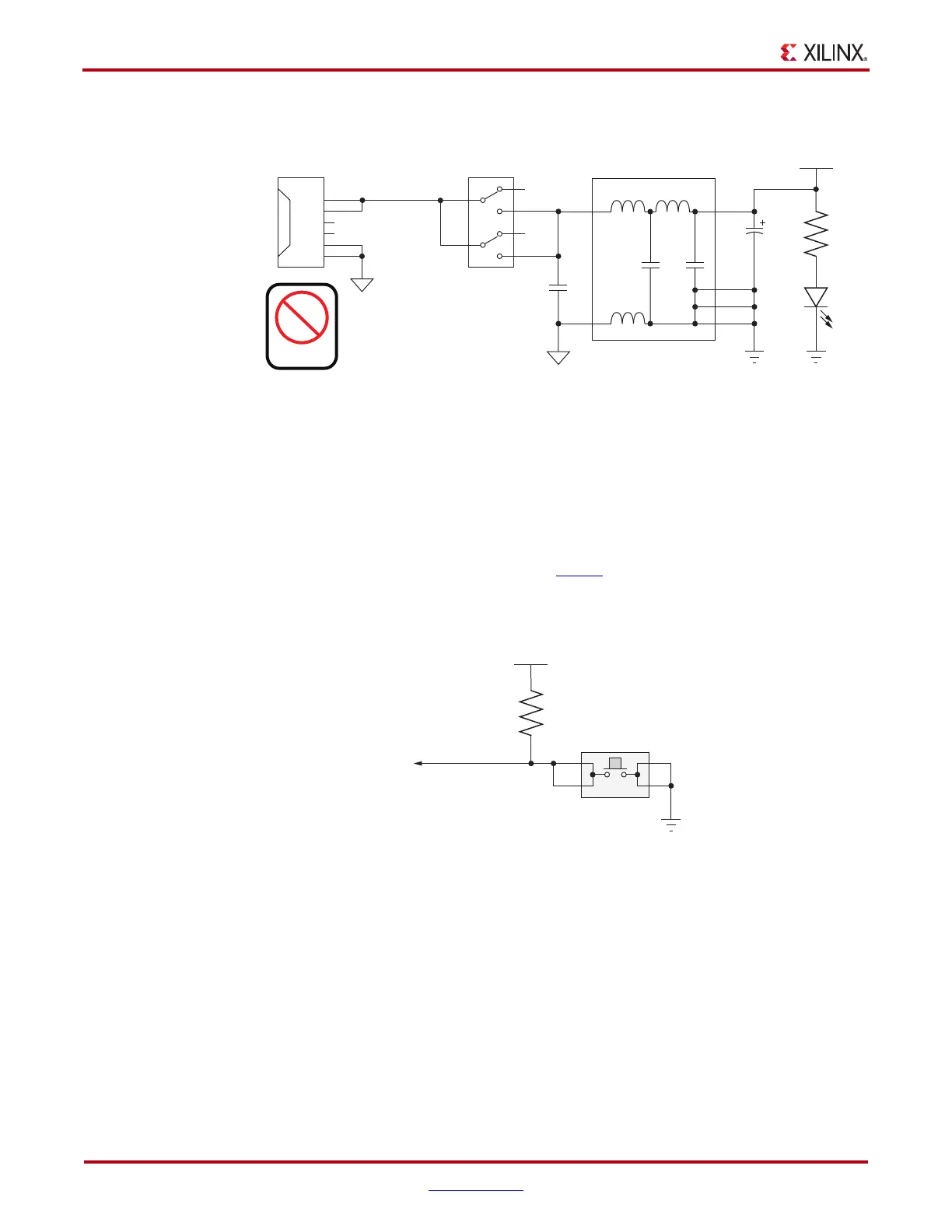
Figure 1-21 shows the power connector J18, power switch SW12, and indicator LED DS16.
FPGA_PROG_B Pushbutton SW9 (Active-Low)
[Figure 1-2, callout 19]
Switch SW9 grounds the FPGA's PROG_B pin when pressed. This action initiates an FPGA
reconfiguration. The FPGA_PROG_B signal is connected to FPGA U1 pin AJ11.
See 7 Series FPGAs Configuration User Guide (UG470
) for further details on configuring the
7 series FPGAs.
Figure 1-22 shows SW9.
Configuration Mode and Upper Linear Flash Address Switch (SW11)
[Figure 1-2, callout 20]
FPGA Configuration Mode: DIP switch SW11 positions 3, 4, and 5 control which
configuration mode is used at power-up or when the PROG pushbutton is pressed.
Linear BPI Flash Upper Addresses: DIP switch SW11 positions 1 and 2 control the setting
of address bits FLASH_A25 and FLASH_A24. The mode signals FPGA_M2, _M1, and _M0
are connected to FPGA U1 pins AJ10, AK10, and AL10, respectively. Configuration mode is
used at power-up or when the PROG pushbutton is pressed.
X-Ref Target - Figure 1-21
Figure 1-21: Power On/Off Switch SW15
UG887_c1_21_090612
VCC12_P_IN
VCC12_P
R279
1kΩ
1%
INPUT_GND
1
2
3
4
SW12
GND
C320
330μF
25V
C471
1μF
25V
GND
DS16
5
6
J18
1
2
3
4
5
6
12V
N/C
COM
12V
N/C
COM
INPUT_GND
Power
PCIe
U73
1
3
8
7
6
5
X-Ref Target - Figure 1-22
Figure 1-22: FPGA_PROG_B Pushbutton SW9
UG887_c1_22_090612
VCC1V8
FPGA_PROG_B
R42
4.7kΩ
0.1 W
5%
GND
1
2 3
4
SW9