60 www.xilinx.com VC709 Evaluation Board
UG887 (v1.0) February 4, 2013
Chapter 1: VC709 Evaluation Board Features
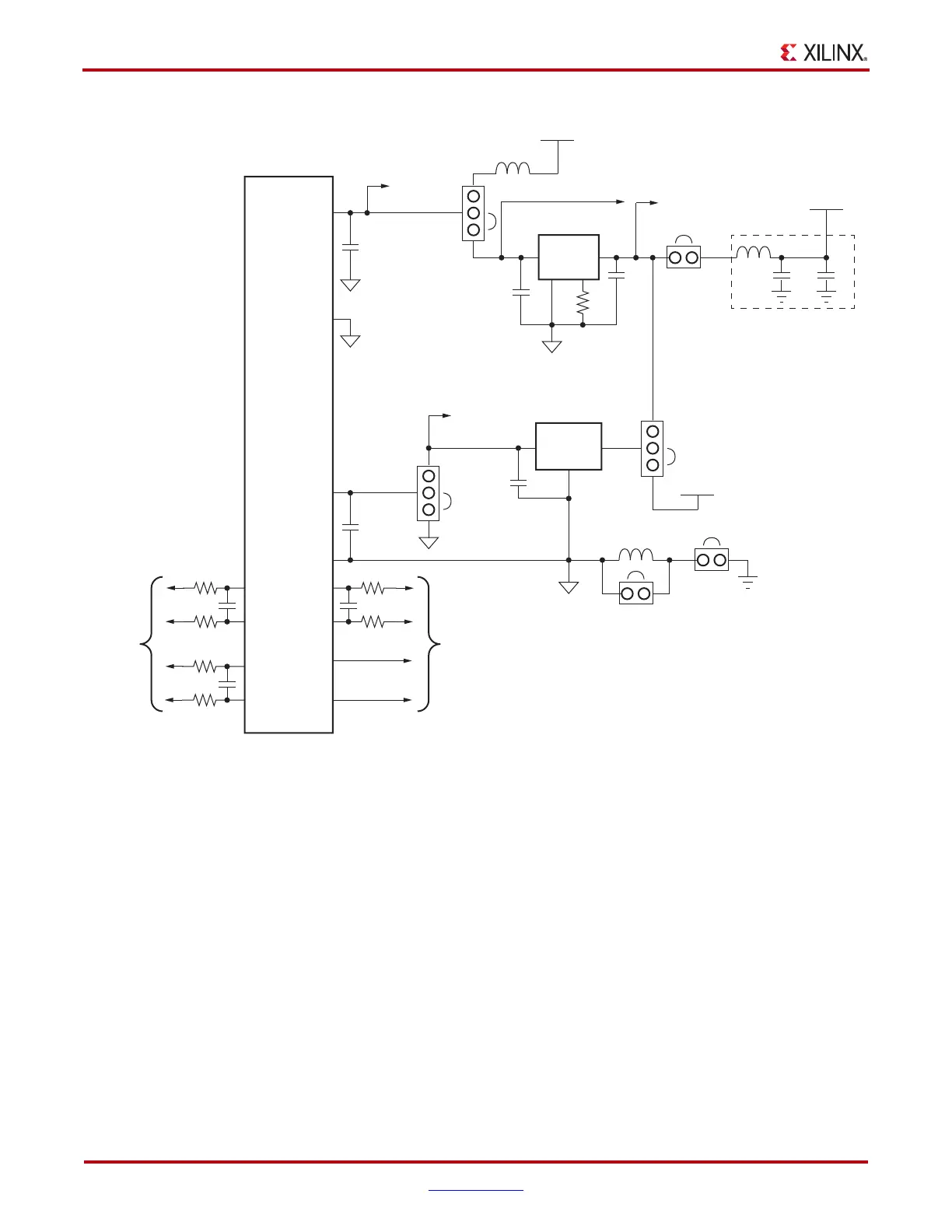
The VC709 board supports both the internal FPGA sensor measurements and the external
measurement capabilities of the XADC. Internal measurements of the die temperature,
V
CCINT
, V
CCAUX
, and V
CCBRAM
are available. The VC709 board V
CCINT
and V
CCBRAM
are
provided by a common 1.0 V supply.
Jumper J42 can be used to select either an external differential voltage reference (VREF) or
on-chip voltage reference for the analog-to-digital converter.
For external measurements an XADC header (J19) is provided. This header can be used to
provide analog inputs to the FPGA's dedicated VP/VN channel, and to the
VAUXP[0]/VAUXN[0], VAUXP[8]/VAUXN[8] auxiliary analog input channels.
Simultaneous sampling of Channel 0 and Channel 8 is supported.
A user-provided analog signal multiplexer card can be used to sample additional external
analog inputs using the 4 GPIO pins available on the XADC header as multiplexer address
lines. Figure 1-26 shows the XADC header connections (Figure 1-2, callout 23).
Note:
.VADJ is fixed at 1.8V on the VC709 board.
X-Ref Target - Figure 1-25
Figure 1-25: XADC Block Diagram
FPGA
U1
VAUX0N
VAUX0P
VAUX8N
VAUX8P
V
REF (1.25V)
V
REFN
VCCADC
GNDADC
V
N
V
P
DXP
DXN
UG887_c1_25_011013
100Ω
1 nF
100Ω
100Ω
1 nF
100Ω
To
Header
J19
Dual Use IO
(Analog/Digital)
100Ω
1 nF
100Ω
To
Header
J19
100 nF
XADC_AGND
REF3012
U35
OutIn
Gnd
J42
XADC_AGND
Internal
Reference
To Header J19
10 μF
Ferrite Bead
100 nF
1 nF
Ferrite Bead
J10
J9
Star Grid
Connection
J54
XADC_VCC
XADC_AGND
GND
V
REFP
V
REFP
ADP123
U10
Out
In
Gnd
XADC_AGND
1 μF
XADC_VCC Header J49
100 nF
XADC_AGND
To J54.3
XADC_VCC
J43
Ferrite Bead
VCCAUX
VCC5V0
10 μF
AV_5V To Header J19
1.8V 150 mV max
J53
Filter 5V Supply
Locate Components on Board
Close to
Package Pins
Close to
Package Pins