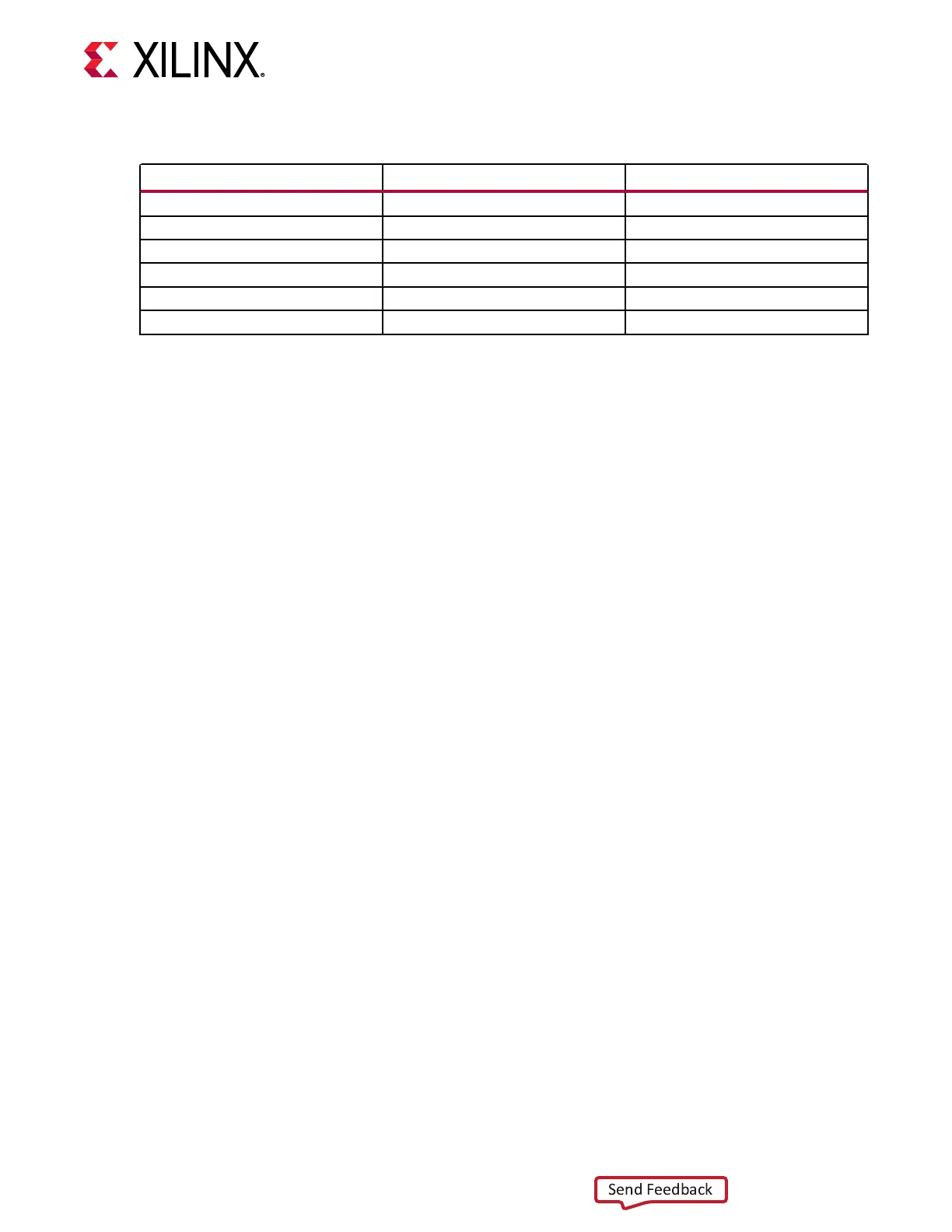
Table 5: I/O Bank Voltage Rails (cont'd)
FPGA (U1) Bank Power Supply Rail Net Name Voltage
HP bank 72 VADJ 1.8V
HP bank 73 RLD3_VDDQ_1V2 1.2V
HP bank 74 RLD3_VDDQ_1V2 1.2V
HP bank 75 RLD3_VDDQ_1V2 1.2V
HBM_43 (not used) VCCHBM/VCCAUX_HBM 1.2V/1.8V
HBM_83 (not used) VCCHBM/VCCAUX_HBM 1.2V/1.8V
DDR4 Component Memory
[Figure 2, callout 4]
The 4.5 GB DDR4 component memory system is comprised of ve 512 Mb x 16 DDR4 SDRAM
devices implemented in clam-shell fashion located at U17-U19 (top) and U73-U74 (boom). Half
of the U19 16-bits are used (4.5 x 16-bits = 72-bit wide interface).
• Manufacturer: Micron
• Part Number: MT40A512M16LY-075E
• Descripon:
○ 8 Gb (512 Mb x 16)
○ 1.2V 96-ball TFBGA
○ DDR4-2666
The VCU128 XCVU37P FPGA DDR4 interface performance is documented in the Virtex
UltraScale+ FPGA Data Sheet: DC and AC Switching Characteriscs (DS923).
The 72-bit wide DDR4 memory system is connected to XCVU37P U1 HP banks 64, 65 and 66.
The DDR4 0.6V VTT terminaon voltage (net DDR4_VTERM_0V6) is sourced from the TI
TPS51200DR linear regulator U71. The DDR4 memory interface bank VREF pins are not
connected, which, coupled with an XDC set_property INTERNAL VREF constraint, invoke the
INTERNAL VREF mode. The connecons between the 72-bit interface DDR4 component
memories and XCVU37P banks 64, 65, and 66 are listed in the following table.
Chapter 3: Board Component Descriptions
UG1302 (v1.0) December 21, 2018 www.xilinx.com
VCU128 Board User Guide 20