Chapter 1
Introduction
Overview
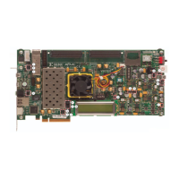
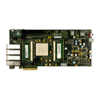
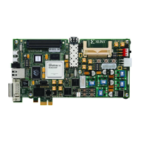
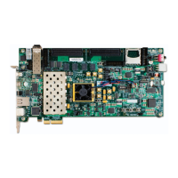
The VCU128 board incorporates the VU37P high bandwidth memory (HBM) FPGA, which
ulizes stacked silicon interconnect (SSI) technology to add HBM die next to the FPGA die on the
package substrate. The VCU128 evaluaon board for the Xilinx
®
Virtex
®
UltraScale+™ FPGA
provides a hardware environment for developing and evaluang designs targeng the UltraScale
+ XCVU37P-2FSVH2892E device. The VCU128 evaluaon board is equipped with many of the
common board-level features needed for design development as listed here.
• DDR4, RLD-3, and QDR-IV component memory
• Ganged small form-factor pluggable (QSFP28) connectors
• Sixteen-lane PCI Express
®
interface
• Ethernet PHY
• General purpose I/O
• UART interface
Addional features can be supported using modules compable with the VITA-57.4 (FMCP
HSPC) connector on the VCU128 board.
Additional Resources
See Appendix D: Addional Resources and Legal Noces for references to documents, les, and
resources relevant to the VCU128 evaluaon board.
UG1302 (v1.0) December 21, 2018 www.xilinx.com
VCU128 Board User Guide 5
 Loading...

