Do you have a question about the Xilinx SP605 and is the answer not in the manual?
Lists chapters and appendices in the manual.
Lists related documents for download.
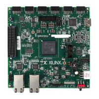
Introduces the SP605 board and its purpose.
Lists resources available for the SP605 board.
Lists the key hardware features of the SP605 board.
Provides a high-level block diagram of the SP605.
Lists resources for additional Xilinx documentation.
Provides essential ESD prevention procedures.
Describes the main FPGA chip on the SP605 board.
Explains the voltage rails for the FPGA I/O banks.
Details the DDR3 memory module on the board.
Explains the SPI flash memory for configuration.
Describes the Linear BPI flash memory.
Covers the System ACE CF controller and CF card slot.
Details the USB-to-JTAG interface for configuration.
Explains the clock sources available on the board.
Describes the MGTs for high-speed serial communication.
Details the PCIe interface on the board.
Describes the SFP connector for network modules.
Explains the Ethernet PHY.
Covers the USB-to-UART serial interface.
Describes the DVI video output connector.
Explains the IIC communication interfaces.
Details the general status LEDs on the board.
Describes specific LEDs for Ethernet status.
Explains LEDs related to FPGA configuration status.
Introduces general-purpose user I/O capabilities.
Covers the various switches on the board.
Describes the FMC connector.
Covers board power supply details.
Lists the methods for configuring the FPGA.
Lists default settings for DIP switches.
Lists default settings for jumpers.
Introduces XDC file templates for the SP605.
Lists relevant EU directives.
Lists relevant CE standards.
Details EMC requirements and classification.
Lists safety standards.
| Brand | Xilinx |
|---|---|
| Model | SP605 |
| Category | Motherboard |
| Language | English |
