16 www.xilinx.com SP605 Hardware User Guide
UG526 (v1.9) February 14, 2019
Chapter 1: SP605 Evaluation Board
I/O Voltage Rails
There are four available banks on the XC6SLX45T-3FGG484 device. Banks 0, 1, and 2 are
connected for 2.5V I/O. Bank 3 is used for the 1.5V DDR3 component memory interface of
Spartan-6 FPGA’s hard memory controller. The voltage applied to the FPGA I/O banks
used by the SP605 board is summarized in Table 1-2.
See the X
ilinx Spartan-6 FPGA documentation for more information.
2. 128 MB DDR3 Component Memory
The SP605 128 MB 16-bit wide DDR3 memory consists of a single 1 Gb x 16 SDRAM U42
wired to Bank 3 (V
cco
= 1.5V) of the U1 XC6SLX45T FPGA. The Spartan-6 FPGA hard
memory controller is used for data transfer across the DDR3 memory interface’s 16-bit
data path using SSTL15 signaling.
•Manufacturer: Micron
• Part Number: MT41J64M16LA-187E
•Description:
• 1 Gb: 128 MB (64 Mb x 16)
• 1.5V 96-ball FBGA
• Performance: up to DDR3-1066
The SP605 board supports the “standard” VCCINT setting of 1.20V ± 5%. This setting
provides memory controller block (MCB) performance of 667 MT/s for DDR3 memory.
The SP605 XC6SLX45T FPGA DDR interface performance is documented in the Spartan-6
FPGA Data Sheet: DC and Switching Characteristics (DS162). [Ref 1]
Signal integrity is maintained through DDR3 resistor terminations and memory on-die
terminations (ODT), as shown in Table 1-3 and Table 1-4.
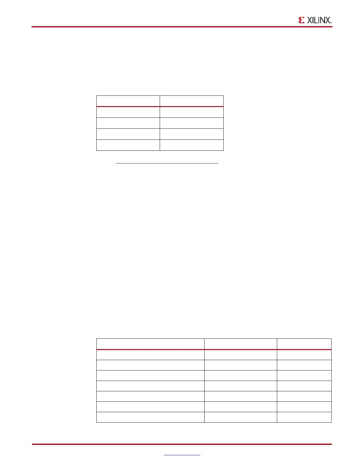
Table 1-2: I/O Voltage Rail of FPGA Banks
FPGA Bank I/O Voltage Rail
02.5V
12.5V
22.5V
31.5V
Table 1-3: Termination Resistor Requirements
Signal Name Board Termination On-Die Termination
MEM1_A[14:0] 49.9Ω to V
TT
–
MEM1_BA[2:0] 49.9Ω to V
TT
–
MEM1_RAS_N 49.9Ω to V
TT
–
MEM1_CAS_N 49.9Ω to V
TT
–
MEM1_WE_N 49.9Ω to V
TT
–
MEM1_CS_N 100Ω to GND –
MEM1_CKE 4.7 KΩ to GND –