Do you have a question about the Xilinx KC705 and is the answer not in the manual?
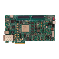
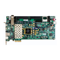
Overview of the KC705 board, its purpose, and key features.
Central FPGA and its DDR3/Flash memory interfaces.
Clock sources and serial transceivers (GTX, PCIe).
Interfaces for Ethernet, USB-UART, HDMI, LCD, I2C, and FMC.
Pinout for the FMC High Pin Count connector.
| FPGA Speed Grade | -2 |
|---|---|
| Package | FFG900 |
| Logic Cells | 326, 080 |
| DSP Slices | 840 |
| Transceivers | 16 |
| Flash Memory | 128 MB |
| Form Factor | ATX |
| FPGA Device | Kintex-7 |
| Configuration | JTAG |
| Ethernet | 10/100/1000 |
| USB | USB |
| Expansion Connectors | FMC |
| PCIe | PCIe Gen2 |
| Clock Sources | 200MHz oscillator |
| Power Supply | 12V |
| Clocking | Fixed 200MHz oscillator |


