KC705 Evaluation Board 31
UG810 (v1.8) March 20, 2018 www.xilinx.com
Chapter 1: KC705 Evaluation Board Features
termination resistor). The user-provided 2.5V differential clock circuit is shown in
Figure 1-12.
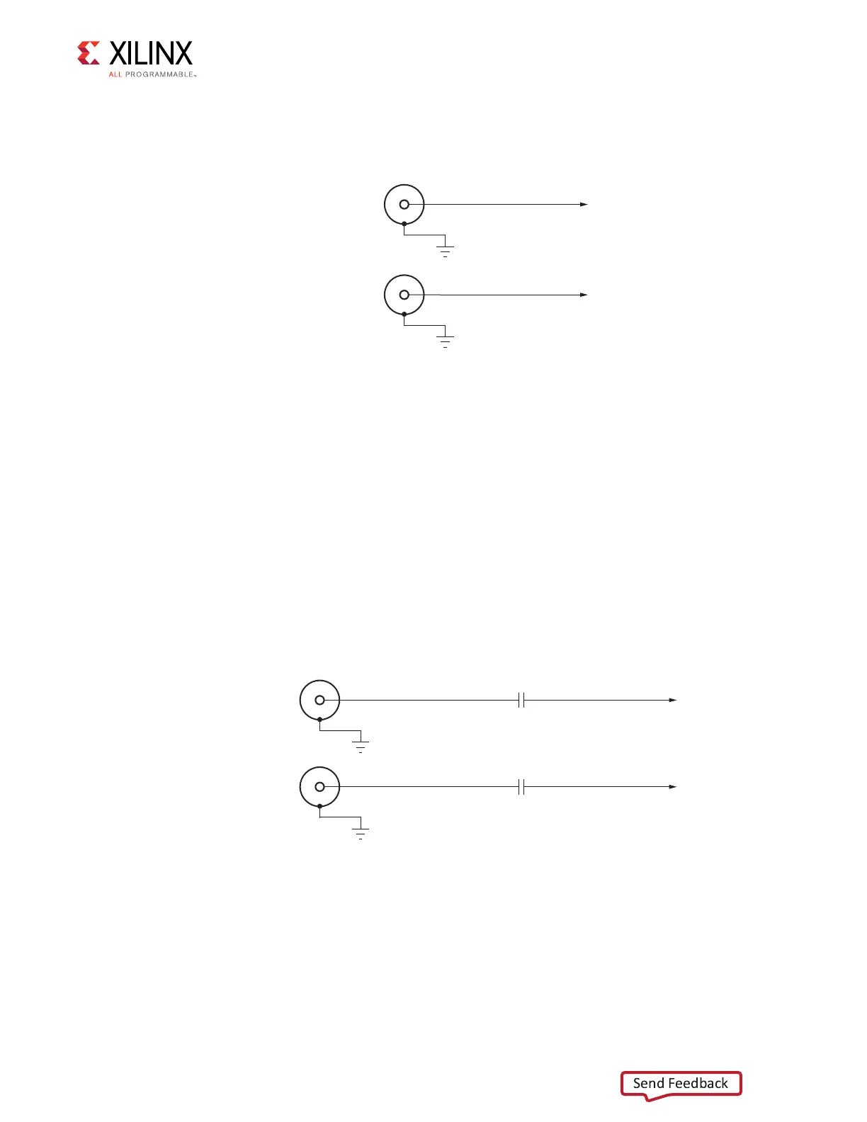
GTX SMA Clock Input
[Figure 1-2, callout 10]
The KC705 board includes a pair of SMA connectors for a GTX clock wired to GTX Quad bank
117. This differential clock has signal names SMA_MGT_REFCLK_P and SMA_REFCLK_N,
which are connected to FPGA U1 pins J8 and J7 respectively. Figure 1-13 shows this
AC-coupled clock circuit.
• External user-provided GTX reference clock on SMA input connectors
• Differential Input
X-Ref Target - Figure 1-12
Figure 1-12: User SMA Clock Source
X-Ref Target - Figure 1-13
Figure 1-13: GTX SMA Clock Source
USER_SMA_CLOCK_P
J12
USER_SMA_CLOCK_N
GND
J11
GND
UG810_c1_12_031214
SMA
Connector
SMA
Connector
UG810_c1_13_031214
SMA_MGT_REFCLK_PSMA_MGT_REFCLK_C_P
SMA
Connector
J16
GND
C11
0.01 μF 25V
X7R
SMA_MGT_REFCLK_NSMA_MGT_REFCLK_C_N
SMA
Connector
J15
GND
C10
0.01 μF 25V
X7R