KC705 Evaluation Board 30
UG810 (v1.8) March 20, 2018 www.xilinx.com
Chapter 1: KC705 Evaluation Board Features
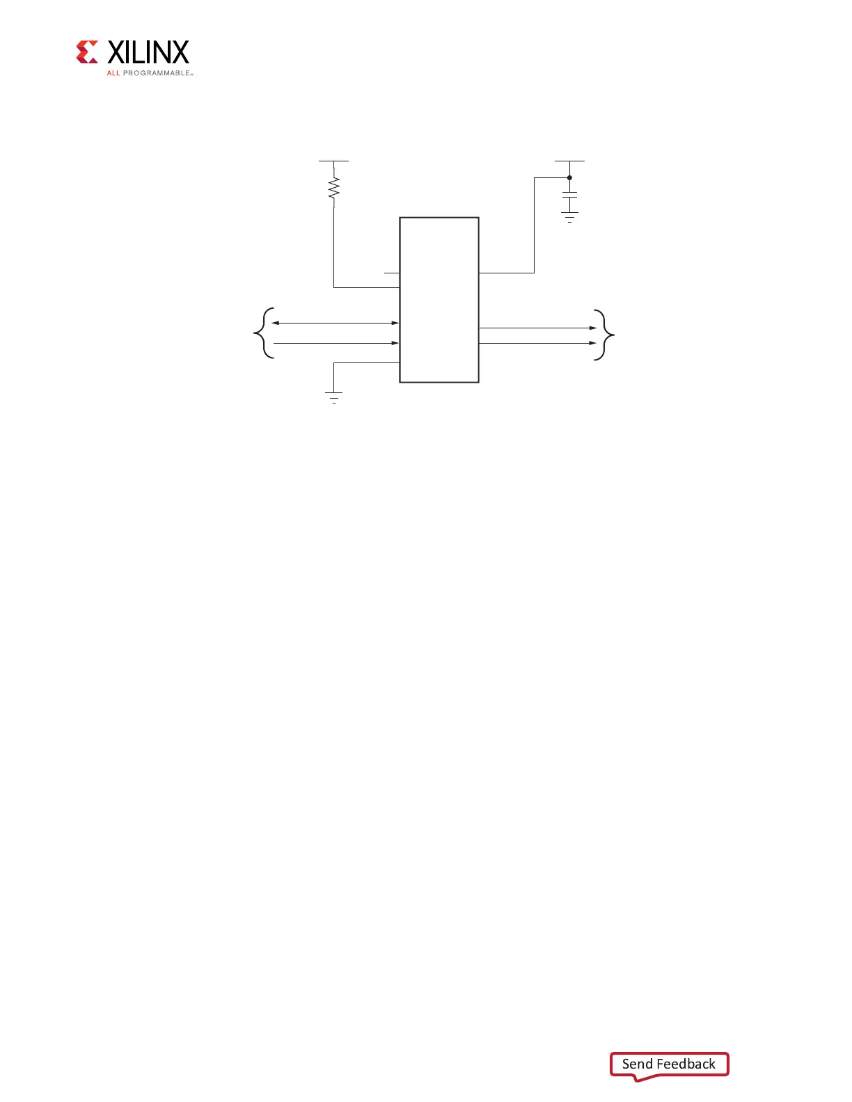
The user clock circuit is shown in Figure 1-11.
For more information about the Silicon Labs Si570 see [Ref 7].
Reference design files are available to demonstrate how to program the Si570
programmable oscillator. See these files and presentations:
• XTP186, KC705 Si570 Programming [Ref 8]
• RDF0175, KC705 Si570 Programming Design Files [Ref 9]
• XTP187, KC705 Si570 Fixed Frequencies [Ref 10]
• RDF0176, KC705 Si570 Fixed Frequencies Design Files [Ref 11]
User SMA Clock Input
[Figure 1-2, callout 9]
An external high-precision clock signal can be provided to the FPGA bank 15 by connecting
differential clock signals through the onboard 50Ω SMA connectors J11 (P) and J12 (N). The
differential clock has signal names are USER_SMA_CLOCK_P and USER_SMA_CLOCK_N,
which are connected to FPGA U1 pins L25 and K25, respectively. J11 (P) and J12 (N) are
connected directly to the noted FPGA pins (no series capacitors and no external parallel
X-Ref Target - Figure 1-11
Figure 1-11: User Clock Source
UG810_c1_11_031214
GND
VCC3V3
Si570
Programmable
Oscillator
NC
OE
GND
SCL
SDA
VDD
1
2
3
8
7
6
U45
R8
4.7KΩ 5%
USER CLOCK N
C77
0.01 μF 25V
X7R
CLK-
4
5
GND
VCC3V3
CLK+
USER CLOCK P
USER CLOCK SDA
USER CLOCK SCL
10 MHz - 810 MHz
50 PPM
To
I
2
C
Bus Switch
(U49)