KC705 Evaluation Board 14
UG810 (v1.8) March 20, 2018 www.xilinx.com
Chapter 1: KC705 Evaluation Board Features
DDR3 Memory Module
[Figure 1-2, callout 2]
The memory module at J1 is a 1 GB DDR3 small outline dual-inline memory module
(SODIMM). It provides volatile synchronous dynamic random access memory (SDRAM) for
storing user code and data.
• Part number: MT8JTF12864HZ-1G6G1 (Micron Technology)
• Supply voltage: 1.5V
• Datapath width: 64 bits
• Data rate: Up to 1,600 MT/s
The DDR3 interface is implemented across I/O banks 32, 33, and 34. Each bank is a 1.5V
high-performance (HP) bank. The VRP/VRN DCI resistor connection to bank 33 is cascaded
to the data interface banks 32 and 34 by adding the DCI cascade constraint to the XDC:
# Set DCI_CASCADE
set_property slave_banks {32 34} [get_iobanks 33]
An external 0.75V reference VTTREF is provided for data interface banks 32 and 34. Any
interface connected to these banks that requires a reference voltage must use this FPGA
voltage reference. The connections between the DDR 3 memory and the FPGA are listed in
Table 1-4.
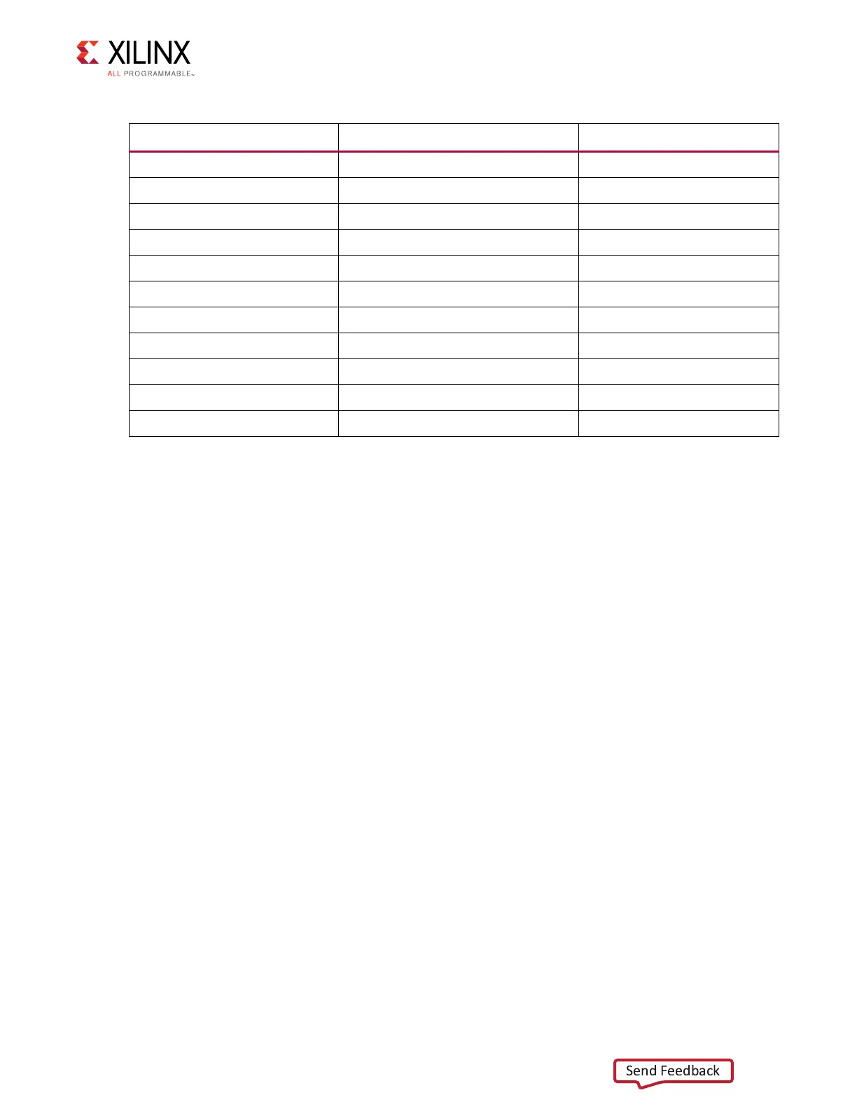
Table 1-3: I/O Voltage Rails
U1 FPGA Bank Power Supply Rail Net Name Voltage
Bank 0 VCC2V5_FPGA 2.5V
Bank 12
(1)
VADJ_FPGA 2.5V (default)
Bank 13
(1)
VADJ_FPGA 2.5V (default)
Bank 14 VCC2V5_FPGA 2.5V
Bank 15 VCC2V5_FPGA 2.5V
Bank 16
(1)
VADJ_FPGA 2.5V (default)
Bank 17
(1)
VADJ_FPGA 2.5V (default)
Bank 18
(1)
VADJ_FPGA 2.5V (default)
Bank 32 VCC1V5_FPGA 1.5V
Bank 33 VCC1V5_FPGA 1.5V
Bank 34 VCC1V5_FPGA 1.5V
Notes:
1. The VADJ_FPGA rail can support 1.8V, 2.5V, or 3.3V. For more information on VADJ_FPGA see Power Management,
page 71.